
TMM6 Filter-Leiterplattenfertigung
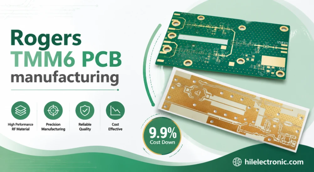
Die Fertigung von TMM6-Filter-Leiterplatten wird durch die Geometrie des fertigen Resonators und der Kopplung bestimmt. Die gewählte Güteklasse ermöglicht ein kompaktes Design, die Filtercharakteristik hängt jedoch weiterhin davon ab, wie genau die Leiterplatte die simulierten Abmessungen wiedergibt. Ein Mikrowellenfilter ist eine elektrische Struktur, die aus physikalischen Abmessungen besteht. Bei einer Rogers TMM6-Leiterplatte beeinflussen Resonatorlänge, Leiterbahnbreite, Kopplungsspalt, Dielektrikumdicke, Kupferprofil, Platzierung der Durchkontaktierungen und Steckverbinderübergänge die gemessene Filtercharakteristik.
TMM6 weist einen Prozess-Dk-Wert von 6.00 ±0.080, einen Design-Dk-Wert von 6.3 und einen typischen Df-Wert von 0.0023 auf. Sein Dk-Bereich ermöglicht kompakte Filter und HF-Netzwerke, ohne dass man sofort zu der viel kleineren Geometrie eines Dk-Werts nahe 10 übergehen muss.
Projektübersicht auf einen Blick
| Optimale Bildschirmwahl | Mikrowellenfilter und kompakte HF-Netzwerke, bei denen ein Dk-Wert nahe sechs eine Größenreduzierung ermöglicht, ohne auf die kleinste Geometrie mit hohem Dk-Wert zurückgreifen zu müssen. |
|---|---|
| Hauptrisiko bei der Herstellung | Durch die Linienbreite, den Kopplungsspalt, die Resonatorlänge, die Dicke des Dielektrikums, das Kupferprofil, die Platzierung der Durchkontaktierungen oder die Variation der Steckverbinderanbindung kann es zu einer Verschiebung des Durchlassbereichs kommen. |
| Erwartete technische Leistung | Ein kontrollierter physischer Fertigungsdatensatz, der CAM-Abmessungen, Prüfdaten, Montageanweisungen und die vom Kunden definierte VNA-Abnahmemethode miteinander verbindet. |
Die Seite zum TMM6-Filter konzentriert sich auf die Resonator- und Kopplungsgeometrie. Fertigungsprüfungen sollten diese HF-Abmessungen mit den galvanisch abgegrenzten Übergängen, den Erstmustermessungen und der für die Serienproduktion festgelegten Konstruktion verknüpfen.
Warum Entwickler von Mikrowellenfiltern TMM6 verwenden
TMM6 ermöglicht im Vergleich zu Laminaten mit niedrigerem Dk-Wert eine Reduzierung der Resonator- und Anpassungsnetzwerkgröße bei gleichzeitig besser herstellbaren Abmessungen als Designs mit sehr hohem Dk-Wert. Rogers gibt zudem einen Wärmeausdehnungskoeffizienten (Dk) von −11 ppm/°C und kupferangepasste CTE-Eigenschaften an, was insbesondere dann von Vorteil ist, wenn elektrische Stabilität und die Zuverlässigkeit der durchkontaktierten Löcher wichtig sind.
Das Material basiert auf einem Duroplast, ist kriech- und kaltflussbeständig und kann mit gängigen Leiterplattenverfahren verarbeitet werden. Diese Kombination ist attraktiv für Filter, die in bearbeitete Gehäuse eingebaut, mit SMA- oder SMP-Schnittstellen verbunden oder mit aktiven Bauelementen kombiniert werden müssen.
Highleap kann TMM6-Platinen im Rahmen unseres umfassenderen TMM-Hochfrequenzprogramms herstellen.
TMM6 vs. TMM10 für Filtergröße und Toleranz
| Entscheidungsfaktor | TMM6 | TMM10 | Auswirkungen auf die Filterkonstruktion |
|---|---|---|---|
| Prozess Dk | 6.00 ± 0.080 | 9.20 ± 0.230 | TMM10 ermöglicht kleinere Resonatoren; TMM6 ermöglicht größere, oft leichter zu kontrollierende Geometrien. |
| Design Dk | 6.3 | 9.8 | Für beide Materialien muss ein Filter neu konstruiert werden. |
| Typischer Df | 0.0023 | 0.0022 | Die veröffentlichten dielektrischen Verluste liegen nahe beieinander; die Leiterverluste und die Geometrie können das Ergebnis bestimmen. |
| Thermischer Koeffizient von Dk | −11 ppm/°C | −38 ppm/°C | Beide Werte sind negativ; die vollständige Temperaturreaktion sollte auf Schaltungsebene ausgewertet werden. |
| Fertigungssensibilität | Mäßig hohe Dk-Geometrie | Stärkere Miniaturisierung und engere absolute Abmessungen | TMM6 bietet möglicherweise ein besseres Verhältnis von Ausbeute zu Leistung, bei dem ein maximaler Schrumpf nicht erforderlich ist. |
Das beste Filtermaterial ist nicht immer das mit dem höchsten Dk-Wert. Wenn TMM10 nur geringfügig Fläche einspart, aber den Kopplungsspalt in einen schwer tolerierbaren Bereich verschiebt, kann TMM6 ein reproduzierbareres Produkt liefern. Unsere Hinweise zur Umrechnung elektrischer Empfindlichkeiten in realistische Fertigungstoleranzen sind in dieser Phase hilfreich.
Typische TMM6-Anwendungen jenseits von Filtern
| Anwendung | Warum TMM6 passt | Primärproduktionsbelange |
|---|---|---|
| Duplexer und Diplexer | Kompakte Resonatoren und mehrere gekoppelte Abschnitte. | Kanal-zu-Kanal-Isolation, Wechselwirkung der Kavität und Dimensionskorrelation. |
| Leistungsteiler und -kombinierer | Kontrollierte Impedanz und elektrische Länge in einem kompakten Netzwerk. | Amplituden-/Phasenausgleich durch Erdung und Steckverbindersymmetrie. |
| Anpassungsplatinen für Leistungsverstärker | Durch die Verwendung von High-Dk-Anpassungsabschnitten kann die Modulgröße reduziert werden. | Thermischer Pfad, Strombelastbarkeit, Oberflächenbeschaffenheit und Erdungsinduktivität. |
| Radar- und Mikrowellen-Frontends | Stabile HF-Verbindungen in kompakten Modulen. | Wiederholbarkeit des Startvorgangs, Abschirmung, Materialchargen- und Temperaturverhalten. |
| Miniaturantennenzuführungen | Verringerte Zuführungsnetzwerkfläche im Vergleich zu Laminaten mit niedrigem Dk-Wert. | Antenneneffizienz, Speiseverluste, Maske und Abstimmungszugriff. |
Das Layout sollte auch festlegen, wo die RF-Masse-Vias hingehören und wie sich der Rückweg auf die Signalintegrität auswirkt , anstatt diese Entscheidungen dem CAM zu überlassen.
Welche Dimensionen beeinflussen die Mittenfrequenz eines Filters?
Die relevanten Dimensionen hängen von der Topologie ab, aber die folgenden Merkmale dominieren im Allgemeinen:
- Elektrische Länge und offene Geometrie des Resonators;
- Kopplungslücken zwischen benachbarten Leitungen oder Resonatoren;
- fertige dielektrische Dicke zwischen der Schaltungs- und der Referenzebene;
- Fertige Kupferdicke und geätzte Seitenwandgeometrie;
- Abstand über den Zaun, Durchmesser des Zauns und Rückweg über den Boden;
- Position der Anschlussstifte, Übergang zwischen Startrampe und Referenzebene;
- Nähe zum Gehäuse, Abmessungen des Hohlraums und Montagedruck.
In einer Fertigungszeichnung sollten diese funktionalen Maße von den üblichen mechanischen Maßen unterschieden werden. Der Filter ist nicht zielführend, wenn zwar alle Konturmerkmale eng toleriert sind, der Resonanzspalt aber nur allgemein angegeben wird.

Materialumfang: Die Rogers-Produktbezeichnung dient zur Identifizierung des für die Leiterplattenfertigung spezifizierten Laminats. Highleap Electronics übernimmt die Leiterplattenfertigung und -bestückung, während das Laminat separat beschafft und geprüft wird.
Wie Highleap einen TMM6-Filteraufbau steuert
- Die elektrische Anlage einfrieren: TMM6-Dicke, Kupfer, Referenzebene und Design Dk bestätigen.
- Kennzeichnen Sie die HF-kritische Geometrie: Identifizieren Sie Resonator-, Spalt-, Start- und Bodenmerkmale, die das Durchlassband beeinflussen.
- Vorgeschlagene Endabmessungen zurückgeben: Die CAM-Kompensation muss unter Berücksichtigung der angestrebten Kupfergeometrie angewendet werden.
- Ausrichtung des Planpanels und Coupons: Platzieren Sie repräsentative Merkmale und Impedanzstrukturen dort, wo sie die Produktionsbedingungen widerspiegeln.
- Vor der Montage prüfen: Messen Sie ausgewählte Linienbreiten, Abstände, Platinendicke, Konturen und PTH-Qualität.
- Schnittstellen der Steuerbaugruppe: Steckverbinder, Schirmungen und Gehäuse so ausrichten, dass die HF-Struktur nicht verzerrt wird.
- Korrelieren Sie die HF-Daten: Vergleichen Sie die Ergebnisse von VNA- oder Modultests mit den genehmigten physikalischen Messungen.
Dieser gezielte Fertigungsablauf unterscheidet sich von einem herkömmlichen Leiterplattenfertigungsprozess, da er sich an der Übertragungsfunktion des Filters orientiert. Die zugrundeliegenden Steuerungsmechanismen in der Fertigung werden in unserem Abschnitt zur Herstellung von Hochfrequenzplatinen beschrieben.
Erstmusterprüfung: Coupon-, VNA- und mechanische Daten
Ein erster Artikel sollte zwei Fragen beantworten: Wurde die Platine gemäß der genehmigten Geometrie gefertigt, und liefert diese Geometrie das erforderliche HF-Verhalten? Mechanische Daten ohne HF-Daten können ein Modellproblem übersehen lassen; HF-Daten ohne mechanische Daten können zwar einmalig funktionieren, sind aber nicht reproduzierbar.
| Validierungselement | Was es bestätigt | Typischer Datensatz |
|---|---|---|
| Material und Schichtaufbau | Korrekte TMM6-Qualität und fertige dielektrische Konstruktion. | Materialdokument und Querschnitt. |
| Kupfergeometrie | Kritische Breiten, Abstände und Längen liegen innerhalb des funktionalen Bereichs. | Optischer Messbericht. |
| PTH und Erdung | Die Kupfer- und Erdungsrückleitungsstruktur ist physikalisch einwandfrei. | Mikroschnitt- und elektrische Prüfung. |
| Impedanz-Coupon | Die Geometrie der Übertragungsleitung korreliert mit dem Schichtaufbau. | TDR-Bericht im Zusammenhang mit dem Gremium. |
| Filterantwort | Durchlassbereich, Einfügungsdämpfung, Rückflussdämpfung, Sperrdämpfung und Mittenfrequenz erfüllen die Grenzwerte. | VNA-Bericht mit Angaben zu Vorrichtung und Kalibrierung. |
Die Validierung kann S-Parameter- oder andere HF-Messungen auf Platinenebene mit kundenspezifischen Prüfungen an der fertigen Baugruppe kombinieren.
Fehlermodi der Filter-Leiterplatte, die wir vor der Freigabe prüfen
- Das Modell verwendet eine nominelle Dicke, während in der Produktion ein anderer dielektrischer Wert verwendet wird.
- Kopplungsspalte werden durch Ätzkompensation oder Lötstopplack verändert.
- Die Durchkontaktierungen sind zu spärlich oder zu weit vom Resonatorrand entfernt.
- Die Bezugsebene des Steckverbinders ist nicht definiert, wodurch ein Vergleich der Lieferantendaten unmöglich wird.
- Das Gehäuse- oder Schraubenmuster verändert nach der Abstimmung die elektromagnetische Begrenzung.
- Ein Prototyp wird von Hand abgestimmt, die Abstimmungsmethode wird jedoch nicht in eine Produktionsspezifikation übernommen.
- Die VNA-Grenzwerte werden ohne Anweisungen zu Leistungspegel, Vorrichtung, Kalibrierung und Porterweiterung angegeben.
TMM6 Filter-Anfrage-Checkliste
- Exakte Anforderungen an die Dicke von TMM6, die Kupferart und die Oberflächenbeschaffenheit des Kupfers.
- Gerber/ODB++, Bohr-, Fräs- und Fertigungssteuerungszeichnung.
- Kritische Resonator-, Kopplungsspalt- und Einkopplungsabmessungen.
- Genehmigte Stackup- und Impedanztabelle.
- Anforderungen an die Oberflächenbeschaffenheit und die Lötstopplack-Sperrzone.
- Zeichnungen von Steckverbindern, Schirmungen und Gehäusen.
- Ziel-S-Parameter, Frequenzbereich und Akzeptanzgrenzen.
- VNA-Vorrichtung, Kalibrierebene und Testanschlussdefinition.
- Prototypenmenge, Produktionsprognose und erforderliche Berichte.
Vom Filterprototyp zur Serienproduktion
Die Serienproduktion darf nicht allein auf Basis von HF-Messergebnissen freigegeben werden. Die physische Konstruktion und der Messbereich, der diese Ergebnisse lieferte, müssen fixiert werden. Die Dokumentation für die Nachproduktion sollte die genehmigten Materialchargenanforderungen, den Schichtaufbau, die CAM-Abmessungen, die Prüfdaten, die Montageanleitung, die VNA-Methode und die Änderungskontrollregeln enthalten. Die Erstmusterprüfung von Highleap konzentriert sich auf die Resonatorabmessungen, die Leitungskopplung, die galvanisch abgegrenzten Übergänge und alle mechanischen Abstimmungsmerkmale. VNA- oder andere HF-Tests können als Teil des Qualifizierungsprozesses definiert werden, wenn die gemessene Filterantwort das Freigabekriterium ist. Die genauen Materialeigenschaften sollten mit der aktuellen Lieferantendokumentation für die angegebene Güteklasse und Konstruktion abgeglichen werden.
Derselbe kontrollierte Fertigungsdatensatz kann für die erste TMM-Prototypenserie und die Serienproduktion verwendet werden. Bitte senden Sie die Filterdateien und Akzeptanzgrenzen zur Überprüfung.
Fragen zur TMM6-Filterherstellung
Welche Fertigungsvariablen können das Ansprechverhalten eines TMM6-Filters beeinflussen?
Die fertige Resonatorlänge, die Leiterbreite, der Kopplungsspalt, die Dicke des Dielektrikums, das Kupferprofil, die Beschichtung, die Durchkontaktierungsgeometrie, der Steckverbinderübergang, die Lötstoppmaske und die Wechselwirkung mit dem Gehäuse können alle die gemessene Antwort beeinflussen.
Reicht eine Impedanzmessung für eine Mikrowellenfilter-Leiterplatte aus?
Nicht immer. TDR- oder Impedanzcoupon-Daten können den Zustand einer Übertragungsleitung bestätigen, während die Filterleistung normalerweise eine definierte VNA-Vorrichtung, Kalibrierebene, Frequenzbereich und S-Parameter-Grenzwerte erfordert.
Soll der erste TMM6-Build Dimensionsdaten enthalten?
Ja. Die Aufzeichnung der physikalischen Abmessungen, die zum HF-Ergebnis geführt haben, macht Abstimmungsentscheidungen nachvollziehbar und verbessert die Wiederholbarkeit der Produktion.
Kann Highleap Steckverbinder und Schirmungen auf TMM6-Filtern montieren?
Die Montage kann HF-Steckverbinder, Abschirmung, mechanische Bauteile und kundenspezifische Tests umfassen, sofern Zeichnungen, Drehmomentvorgaben, Löt-, Reinigungs-, Vorrichtungs- und Abnahmekriterien vorliegen. Für ein Angebot für einen TMM6-Filter benötigen wir das Frequenzband, die Filterzeichnung, den Lagenaufbau, die Leiterplattendicke, kritische Abmessungen, die Stückzahl und das HF-Testverfahren. So stellen wir sicher, dass die Produktionsplanung den tatsächlichen Abnahmekriterien entspricht.
Verwandte Ressourcen zur Leiterplattenfertigung von Rogers
- Rogers TMM Leiterplattenhersteller & Bestückungslieferant
- Rogers TMM4 Leiterplatte für HF-Module und Filter
- Rogers TMM10 Leiterplattenfertigung für kompakte HF-Designs
- Rogers TMM PCB Preis-, Kostentreiber- und Angebotsleitfaden

Empfohlen Beiträge

TMM3 Leiterplattenfertigung für HF-Module
Die Fertigung von TMM3-Leiterplatten ist am sinnvollsten dort, wo das HF-Modul...

TMM6 Leiterplattenfertigung
TMM6-Fertigung ist die Prozesssteuerungsseite für eine mittlere Dk...

TMM10 Leiterplattenfertigung für kompakte HF-Designs
Inhaltsverzeichnis: Wie TMM10 HF-Strukturen verkleinert – TMM10 vs. ...

TMM10i Leiterplattenfertigung und DFM
Die Leiterplattenfertigung des TMM10i legt einen stärkeren Fokus auf DFM, weil...
So erhalten Sie ein Angebot für Leiterplatten
Wir führen gerne eine DFM/DFA-Analyse für Sie durch und senden Ihnen anschließend einen Bericht zu. Sie können Ihre Dateien sicher über unsere Website hochladen. Für die Erstellung eines Angebots benötigen wir folgende Informationen:
-
- Gerber, ODB++ oder .pcb, Spezifikation.
- Stückliste, wenn Sie eine Montage benötigen
- Die Menge
- Wendezeit
Für PCBA-Dienstleistungen geben Sie bitte Ihre Stückliste (BOM) und alle spezifischen Montageanweisungen an. Wir bieten auch DFM/DFA-Analysen an, um Ihre Designs hinsichtlich Herstellbarkeit und Montage zu optimieren und so einen reibungslosen Produktionsprozess zu gewährleisten.