
Taconic fastRise 27 Prepreg-Leiterplattenbonden und HDI-Fertigungsservice
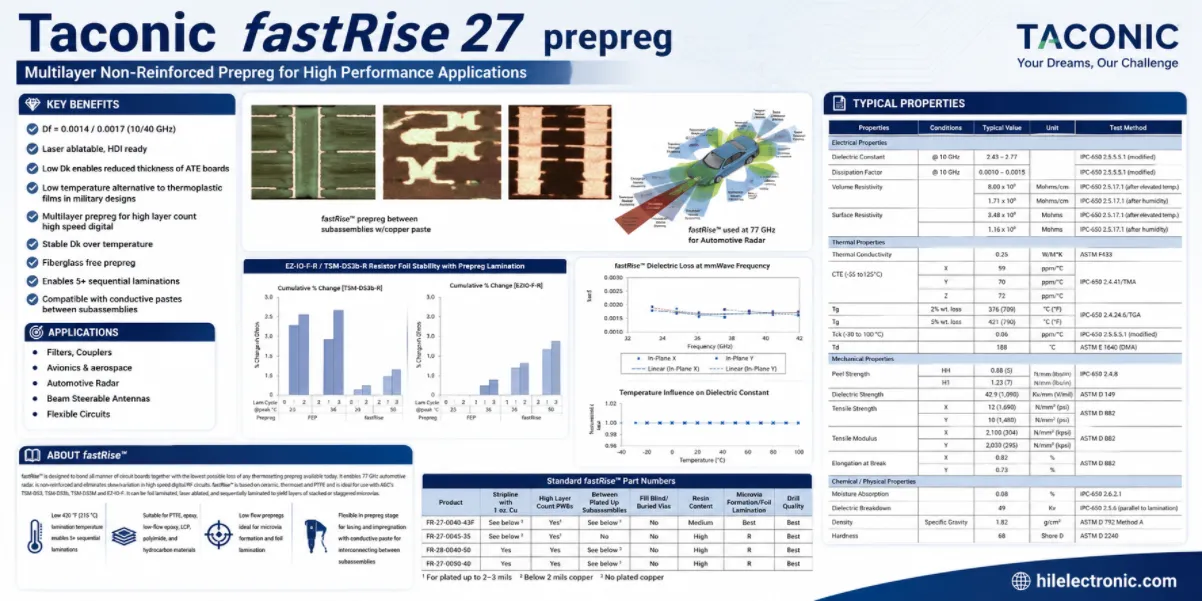
Highleap Electronics prüft Taconic fastRise 27 als Bondmaterial in kompletten HF-Multilayer- oder HDI-Leiterplatten. Wir unterstützen die technische Prüfung hinsichtlich kompatibler Kernmaterialien, Dicke der ausgehärteten Bondlinie, Kupferfüllung, sequenzieller Laminierung , lasergebohrter Mikro-Vias, kontrollierter Impedanz, Montage und kundenspezifischer Qualifizierung.
fastRise 27 Prepreg-Bauumfang
Highleap prüft fastRise 27 im Rahmen der kompletten Multilayer-Prepreg-Konstruktion , einschließlich kompatibler Kerne, Kupferverteilung, Harzbedarf, gepresster Bondline-Ziele, sequenzieller Laminierung, HDI-Stufen und kontrollierter Impedanz. Bei Architekturen mit fortschrittlichen oder beliebigen Layer-Verbindungen werden die gesamte Presssequenz, die Zuverlässigkeit der Mikrovias, die Materialkompatibilität und die Testergebnisse bewertet, bevor der Fertigungsablauf finalisiert wird.
Wichtig: Diese Arbeit dient der Erstellung von Prüfmustern und Qualifizierungsvorlagen sowie der Serienproduktion, sobald die genehmigte Konstruktion finalisiert ist. Eine frühzeitige Überprüfung ist besonders wichtig bei ungewöhnlichen Klebeverbindungen, mehreren Presszyklen, dichtem Kupfer oder hohen Zuverlässigkeitsanforderungen.
Optimale Bildschirmwahl
Verlustarme HF-Mehrschichtsysteme, glasfaserfreie Klebeverbindungen, TSM-DS3-Konstruktionen, Hybridplatinen, lasergebohrtes HDI und sequentielle Laminierung.
Primäres Risiko
Annahme, dass die nominelle Blechdicke zur endgültigen dielektrischen Dicke wird, ohne die Kupfertopographie und den Harzfluss zu analysieren.
Highleap-Scope
Kompatibilitätsprüfung, Klebenaht- und Pressentechnik, sequentielle Laminierung, Bohren/Beschichten, Impedanzkontrolle, Montage und Zuverlässigkeitsprüfung.
Zitat-Eingaben
Oberflächenmaterialien, fastRise-Code, Lagenanzahl, Kupferbelegung, Pressdicke, Pressreihenfolge, Mikrovias, Panel, Menge, PCBA und Qualifizierungsdateien.
Was fastRise 27 ist – und was Sie tatsächlich kaufen
Taconic fastRise FR-27-0040-43F ist ein verlustarmes, nicht verstärktes Prepreg, das zum Verkleben kompatibler Kerne in HF-, Mikrowellen-, Millimeterwellen- und sequenziell laminierten Leiterplatten verwendet wird. AGC gibt für die genannte Konstruktion einen nominalen Dk-Wert von 2.77, einen Df-Wert von 0.0014, eine Glasübergangstemperatur (Tg) von ca. 188 °C und eine Wärmeleitfähigkeit von ca. 0.25 W/m·K an.
Es handelt sich nicht um einen eigenständigen kupferkaschierten Kern, und „fastRise 27 PCB“ ist keine vollständige Produktbeschreibung. Der Kunde erwirbt eine fertige Multilayer-Leiterplatte, deren elektrische Eigenschaften von der ausgehärteten Klebeverbindung zwischen den einzelnen Schichten abhängen. Diese Klebeverbindung entsteht durch den Pressvorgang, die Kupfertopografie, die Lagenanzahl, die Harzbewegung und das Paneldesign.
Verwenden Sie es, wenn
- Verlustarme HF-Kerne benötigen ein kompatibles Bonddielektrikum;
- Glasfasergewebefreie Klebeverbindungen sind wertvoll für schräge oder mmWave-Strukturen;
- Für die Herstellung von sequenziellen Laminierungen oder lasergebohrten Mikrovias sind diese erforderlich;
- Das Projekt ermöglicht die Kontrolle der Kupferfüllung und der Pressdicke.
Geben Sie es nicht allein an, wenn
- Die Deckschichtkernmaterialien sind nicht identifiziert;
- Die Berechnung geht davon aus, dass die Rohblechdicke der ausgehärteten Blechdicke entspricht;
- Die Presssequenz und die kumulative thermische Vorgeschichte sind unbekannt;
- Der Kunde erwartet, dass die Bezeichnung des Prepregs die gesamte Leiterplatte definiert.
Highleap-Fähigkeit für fastRise 27 Multilayer- und HDI-Builds
Highleap kann fastRise 27 als Teil einer kompletten starren HF-Mehrlagen-, Hybrid-Leiterplatten- oder sequenziellen Laminierungsstruktur prüfen. Die Dienstleistung kann Materialverträglichkeitsprüfung, Presskonstruktion, Kupferfüllungsanalyse, Laserbohren, mechanisches Bohren, Durchkontaktierungen, Mikrovias, Impedanzkontrolle, Leiterplattenprüfung, Bauteilbeschaffung, Montage und kundenspezifische Tests umfassen.
| Arbeitspaket | Was Highleap prüft | Warum der Käufer es braucht |
|---|---|---|
| Materialverträglichkeit | Zu berücksichtigen sind die chemische Zusammensetzung des Kerns, der Oberflächenzustand, die Kupferbehandlung, das Aushärtungsfenster, der Wärmeausdehnungskoeffizient und die Lieferantenzulassung. | Verhindert schwache Haftung, Lufteinschlüsse, Verformungen oder unzulässige Materialkombinationen. |
| Klebefugendesign | Lagenaufbau, Kupferverteilung, Harzbedarf, lokale Topographie, Pressdicke, Symmetrie und Impedanzempfindlichkeit. | Wandelt ein nominales Prepreg in einen baubaren dielektrischen Abstand um. |
| Sequentielle Laminierung | Pressstufen, Mikrovia-Stack, Capture-Pads, Füllen, Ausrichten und kumulative Wärmeeinwirkung. | Ermittelt, ob die HDI-Struktur zuverlässig und wiederholbar ist. |
| Bohren und Plattieren | Laserparameter, mechanischer Bohrablauf, Entschmieren/Aktivieren, Kupferabscheidung, Füllen und Querschnittsplan. | Kontrolliert die Zuverlässigkeit von Mikrovia- und plattierten Bohrungen. |
| Montage und Test | Verformung, Reflow-Zählung, Bauteilgehäuse, Röntgenzugang, Temperaturwechseltests, Funktions- oder HF-Tests. | Gewährleistet, dass die laminierte Leiterplatte auch nach der Montage noch geeignet ist. |
Prototypen, Kleinserien und Serienfertigungen können bewertet werden, jedoch müssen die gleichen, für Material und Pressverfahren zugelassenen Annahmen auch für die Serienproduktion gelten. Ein mit einem geeigneten Ersatzmaterial gepresstes Muster erfüllt nicht die Anforderungen des vorgesehenen Designs.
Anforderungen an Pressdicke, Harzfluss und Kupferfüllung
Die Dicke der fertigen Klebefuge ist ein fertigungsbedingtes Ergebnis. Sie variiert mit dem Kupferanteil, der Strukturhöhe, den offenen Bereichen, dem Druck, der Temperatur, dem Vakuum, der Plattengröße, den Trennmitteln und der Menge an Harz, die in lokale Hohlräume fließt. Eine nominelle Prepreg-Dicke reicht daher für eine kontrollierte Impedanz oder einen kontrollierten Hohlraumabstand nicht aus.
Vom Kunden benötigte Daten
- vollständige Schichtgrafiken oder repräsentative Kupferdichtekarten;
- genaue Konstruktion des fastRise-Produkts und vorgeschlagene Lagenanzahl;
- Oberflächenkernmaterialien, Oberflächenbehandlung und Kupferprofil;
- gepresstes dielektrisches Ziel und Toleranz;
- Bereiche mit hohem Kupferanteil, großen Abständen, Hohlräumen, Durchkontaktierungen oder eingebetteten Strukturen;
- Impedanz- und Phasenanforderungen, die von der Klebeverbindung abhängen;
- Plattenabmessungen, Ebenheit, Passgenauigkeit und Verzugsgrenzen.
Highleap kann die Lagenanzahl, die lokale Kupferverteilung, die Pressparameter oder die Schichtdicke anpassen, um eine fertigungsgerechte Konstruktion zu erzielen. Jede Änderung, die das elektrische Modell betrifft, wird vor der Werkzeugfertigung dem Kunden zur Genehmigung vorgelegt.
Sequentielle Laminierung und Microvia-Planung
fastRise 27 ist attraktiv für HDI und wiederholte Laminierung, aber die Aussage „unterstützt sequentielle Laminierung“ bedeutet nicht, dass jede gestapelte Mikrovia-Architektur geeignet ist. Die Zuverlässigkeit hängt vom Via-Durchmesser, der dielektrischen Dicke, dem Capture-Pad, der Kupferfüllung, der versetzten oder gestapelten Anordnung, der Pressreihenfolge und der Anzahl der Temperaturzyklen ab.
- Definiere die Reihenfolge des Layeraufbaus. Zeigen Sie, welche Schichten in den einzelnen Pressphasen vorhanden sind und wann die einzelnen Mikrovias gebohrt, beschichtet und gefüllt werden.
- Berechnung der kumulativen thermischen Geschichte. Bei jedem nachfolgenden Laminierungs- und Montage-Reflow werden die zuvor verwendeten Dielektrika und galvanisch abgeschiedenen Verbindungen erneut erhitzt.
- Überprüfung der Registrierung und der dimensionalen Bewegung. Dünne, nicht verstärkte Klebefugen erfordern kontrollierte Handhabung und Ausrichtung.
- Design-Repräsentanten-Gutscheine. Berücksichtigen Sie den eigentlichen Mikrovia-Stack, die Kupferfüllung, das Dielektrikum und die thermische Belastung.
- Nachweis der Akzeptanz festlegen. Kontinuitätsprüfungen allein reichen möglicherweise nicht aus; definieren Sie Querschnittsprüfungen, Temperaturwechselprüfungen, IST-Prüfungen oder andere Zuverlässigkeitsprüfungen, wenn das Produktrisiko dies rechtfertigt.
Die zugehörigen Freigabeanforderungen finden Sie im HDI-Stackup-Leitfaden und den PCB-DFM-Prüfungen von Highleap .
Wo fastRise 27 Mehrwert bietet
77-GHz-Radar-Mehrschichtsysteme
Eine glasfaserfreie Klebeverbindung kann dünne HF-Strukturen und Laserablation unterstützen, aber die angrenzenden Kerne, Antennenschichten, das Kupferprofil und die Messmethode bestimmen weiterhin die mmWellen-Antwort.
TSM-DS3 und andere verlustarme Multilayer
fastRise 27 ermöglicht eine verlustarme und optimal abgestimmte Bondverbindung, sofern die Materialkombination zugelassen ist. Kern und Prepreg müssen als ein dielektrisches System betrachtet werden; ein ähnlicher Dk-Wert beweist keine Kompatibilität.
Hybride HF/Digital-Leiterplatten
Das Prepreg kann zwar die Verbindung von HF-Kernen mit anderen Funktionsschichten erleichtern, jedoch birgt die gemischte chemische Zusammensetzung Risiken hinsichtlich Aushärtung, Wärmeausdehnung, Haftung, Passgenauigkeit und Verzug. Der hybride Schichtaufbau sollte vor der endgültigen Festlegung des Layouts überprüft werden.
Sequentielle Laminierung HDI
Nichtverstärkte Materialien und Laserbearbeitung können Mikrovia-Strukturen ermöglichen. Der wirtschaftliche Nutzen entsteht, wenn HDI ein konkretes Problem bei Durchkontaktierungen, Verbindungen oder HF-Übergängen löst; unnötige Pressvorgänge erhöhen lediglich die Kosten und das Zuverlässigkeitsrisiko.
Kosten- und Terminfaktoren für ein fastRise 27-Projekt
| LED Treiber | Auswirkungen auf den Preis oder die Lieferzeit | Wie man Unsicherheit reduziert |
|---|---|---|
| Genaue Prepreg-Konstruktion und Verfügbarkeit | Sonderbeschaffung, Mindestbestellmenge oder regionale Lieferbedingungen können den Zeitplan beeinflussen. | Bitte prüfen Sie den aktuellen Produktcode und die genehmigte alternative Richtlinie. |
| Lagenanzahl und Pressdicke | Mehrere Lagen, enge dielektrische Toleranzen und Schwankungen im Harzbedarf erhöhen den Entwicklungsaufwand für die Presse. | Kupferkarten und realistische Dickentoleranzen bereitstellen. |
| Anzahl der Presszyklen | Jeder Zyklus birgt zusätzliche Risiken wie Werkzeugaufwand, Registrierung, Inspektion, Materialbewegung und Verbindungsrisiken. | Vereinfachen Sie die HDI-Sequenz, wo immer möglich. |
| Lasergebohrte Mikrovias | Bohren, Beschichten, Füllen, Planarisieren, Röntgen-/Querschnittsprüfung und Zuverlässigkeitsproben verursachen zusätzliche Kosten. | Verwenden Sie Mikro-Vias nur dort, wo dies aufgrund der Breakout- oder HF-Leistung erforderlich ist. |
| Panelgröße und Kupferungleichgewicht | Große oder asymmetrische Platten erhöhen die Verformung und die Dickenabweichung. | Ausgleich des Kupfergehalts und Definition praktischer Anforderungen an die Paneele und deren Ebenheit. |
| Qualifikationsprüfung | IST, Temperaturzyklen, RF-Coupons und Datenberichterstattung verlängern sowohl die Entwicklungs- als auch die Produktionszeit. | Vor der Angebotserstellung sollten der Musterplan und die Bestehens-/Nichtbestehensgrenzen vereinbart werden. |
Die verbindliche Lieferzeit für Leiterplattenlaminate ergibt sich nach Materialbestätigung und Prozessprüfung. Die Angabe der Lieferzeit allein anhand der Prepreg-Bezeichnung ignoriert die Variablen, die den Fertigungsprozess tatsächlich beeinflussen.
Checkliste für Angebotsanfragen zu einem Klebstoffprojekt
Bitte geben Sie den kompletten Schichtaufbau, die genaue fastRise-Produktbezeichnung, die Kernmaterialien, die Lagenanzahl, die Kupfergewichte und -verteilungen, das Ziel der Pressdicke, die Impedanzanforderungen, die Schichtaufbaureihenfolge, die Blind-/Mikrovia-Phasen, den Bohrtisch, die Panelgröße, die Ebenheit, die Registrierung, die Materialrückverfolgbarkeit, die Menge, die Prognose, den Liefertermin und den Qualifizierungsplan an.
Für PCBA sind folgende Angaben erforderlich: Stückliste, Montagezeichnungen, Schwerpunkt, Bauteilverzeichnis, Reflow-Zähler, Platinenstützplan, Reinigungs-/Beschichtungsanforderungen, Inspektion, Funktionstest sowie alle Umwelt- oder Zuverlässigkeitstests.
Das Angebot von Highleap sollte darlegen, was bereits bekannt ist, was noch der Zustimmung des Kunden bedarf und welche Testergebnisse vorliegen. Das ist aussagekräftiger als die allgemeine Zusage, dass das Werk „fastRise unterstützt“.
Verwandte Ressourcen: Hybrid-Leiterplattenlaminierung und Anforderungen an die Impedanzkontrolle.
Häufig gestellte Fragen für Unternehmen
Ist Taconic fastRise 27 ein Laminatkern?
Nein. Es handelt sich um ein nicht verstärktes Prepreg/Bindemittel, das zwischen kompatiblen Leiterbahnmaterialien verwendet wird. Die vollständige Leiterplattenbeschreibung muss die Decklagen, den Lagenaufbau und die Pressdicke angeben.
Kann Highleap mit fastRise 27 sequenzielle Laminierungs- und Mikrovia-Leiterplatten herstellen?
Geeignete Strukturen können geprüft und ein Angebot erstellt werden. Die Machbarkeit hängt von der Schichtfolge, der Dicke des Dielektrikums, der Geometrie der Durchkontaktierungen, der Kupferfüllung, der Passgenauigkeit, den Presszyklen, der Panelgröße und den Zuverlässigkeitsanforderungen ab.
Entspricht die Dicke des unbehandelten Prepregs der Dicke der ausgehärteten Klebefuge?
Nein. Die endgültige Dicke hängt vom Lagenaufbau, der Kupferoberfläche, dem Harzfluss, dem Druck, der Temperatur, dem Vakuum und dem Plattendesign ab. Verwenden Sie einen zugelassenen Produktionsaufbau, nicht nur die Dicke des Rohblechs.
Kann fastRise 27 jeden HF-Kern verbinden?
Nein. Die Kompatibilität muss hinsichtlich Chemie, Oberflächenbehandlung, Aushärtungszyklus, Wärmeausdehnungskoeffizient, Haftung, Kupferbehandlung und Lieferanten-/Kundenfreigabe bestätigt werden.
Was wird für ein Angebot benötigt?
Senden Sie den kompletten Schichtaufbau, die Materialien, die Kupferpläne, die Zielvorgabe für die Pressdicke, die Mikrovia-Sequenz, die Impedanz, die Abmessungen, die Menge, die Lieferbedingungen, das Montagepaket und den Testplan.

Empfohlen Beiträge

TMM4 Filter-Leiterplattenfertigung
Die Herstellung der Leiterplatten für den TMM4-Filter wird gesteuert durch...

TMM3 Leiterplattenfertigung für HF-Module
Die Fertigung von TMM3-Leiterplatten ist am sinnvollsten dort, wo das HF-Modul...

TMM6 Leiterplattenfertigung
TMM6-Fertigung ist die Prozesssteuerungsseite für eine mittlere Dk...

TMM10 Leiterplattenfertigung für kompakte HF-Designs
Inhaltsverzeichnis: Wie TMM10 HF-Strukturen verkleinert – TMM10 vs. ...
So erhalten Sie ein Angebot für Leiterplatten
Wir führen gerne eine DFM/DFA-Analyse für Sie durch und senden Ihnen anschließend einen Bericht zu. Sie können Ihre Dateien sicher über unsere Website hochladen. Für die Erstellung eines Angebots benötigen wir folgende Informationen:
-
- Gerber, ODB++ oder .pcb, Spezifikation.
- Stückliste, wenn Sie eine Montage benötigen
- Die Menge
- Wendezeit
Für PCBA-Dienstleistungen geben Sie bitte Ihre Stückliste (BOM) und alle spezifischen Montageanweisungen an. Wir bieten auch DFM/DFA-Analysen an, um Ihre Designs hinsichtlich Herstellbarkeit und Montage zu optimieren und so einen reibungslosen Produktionsprozess zu gewährleisten.