
HDI PCB για Ρομποτική: Μικροβιακές οπές, BGA Fanout και Ακεραιότητα Σήματος
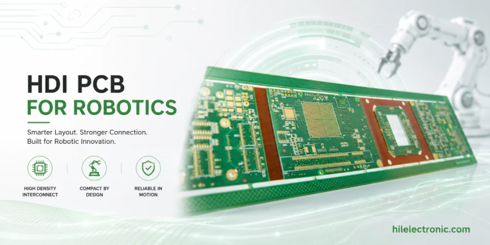
Η κατασκευή PCB HDI για ρομποτική βασίζεται σε συμπαγείς πλακέτες, συσκευές BGA λεπτού βήματος, διεπαφές υψηλής ταχύτητας, πυκνή δρομολόγηση αισθητήρων και στενά μηχανικά περιβλήματα. Οι υπολογιστικές πλακέτες ρομποτικής, οι πλακέτες όρασης, οι ελεγκτές drones, οι ελεγκτές ανθρωποειδών αρθρώσεων και οι συμπαγείς μονάδες επικοινωνίας συχνά δεν μπορούν να δρομολογηθούν μόνο με τυπικές οπές διέλευσης.
Όταν τα ρομποτικά προϊόντα χρειάζονται κατασκευή PCB HDI
BGA με λεπτό βήμα και συμπαγής περιοχή πλακέτας
Το HDI καθίσταται απαραίτητο όταν το βήμα των εξαρτημάτων, η πυκνότητα δρομολόγησης ή η περιοχή της πλακέτας εμποδίζουν την πρακτική εκτροπή των οπών (fanout) με τα τυπικά via. Οι ρομποτικές πλακέτες που χρησιμοποιούν BGA 0.4 mm ή 0.5 mm, οι επεξεργαστές AI, οι επεξεργαστές κάμερας, οι συμπαγείς ασύρματες μονάδες ή τα FPGA με υψηλό αριθμό ακίδων συχνά χρειάζονται μικροvia για να διαφύγουν καθαρά από τα σήματα.
Η HDI δεν πρέπει να επιλέγεται μόνο και μόνο επειδή ακούγεται προηγμένη. Προσθέτει κόστος κατασκευής και πολυπλοκότητα της διαδικασίας. Η βέλτιστη χρήση της HDI είναι στοχευμένη: επίλυση προβλημάτων δρομολόγησης, πυκνότητας ή ακεραιότητας σήματος που η τυπική πολυστρωματική κατασκευή δεν μπορεί να λύσει αξιόπιστα.
Εφαρμογές Ρομποτικής που Χρησιμοποιούν Συνήθως HDI
Το HDI είναι συνηθισμένο στην ρομποτική όραση και τον σχεδιασμό PCB καμερών , PCB υψηλής ταχύτητας για ρομποτική , αρχιτεκτονική PCB ανθρωποειδών ρομπότ και ηλεκτρονικά συμπαγών drones. Αυτά τα προϊόντα συνδυάζουν συσκευασίες λεπτού βήματος με δρομολόγηση υψηλής ταχύτητας, πυκνότητα ισχύος και αυστηρά μηχανικά όρια. Η τυπική κατασκευή μπορεί να επιβάλει μεγαλύτερη πλακέτα ή παραβίαση της δρομολόγησης.
Για μια σελίδα κατασκευής, το κλειδί είναι να εξηγηθεί πώς ο HDI επηρεάζει την κατασκευή, τη συναρμολόγηση, τις δοκιμές και το κόστος. Ένας πελάτης που επιλέγει ένα εργοστάσιο PCB πρέπει να γνωρίζει εάν ο προμηθευτής μπορεί να κατασκευάσει τη δομή με συνέπεια, όχι μόνο να ορίσει τι σημαίνει HDI.
HDI Stackups, Microvias, Via-in-Pad και BGA Fanout
Επιλογές 1-N-1, 2-N-2 και Οποιαδήποτε Στρώση
Οι συνήθεις δομές HDI περιλαμβάνουν 1-N-1, 2-N-2 και HDI οποιουδήποτε επιπέδου. Μια στοίβαξη 1-N-1 μπορεί να λύσει ένα μέτριο πρόβλημα fanout BGA. Μια στοίβαξη 2-N-2 προσφέρει μεγαλύτερη πυκνότητα δρομολόγησης. Η HDI οποιουδήποτε επιπέδου παρέχει την υψηλότερη ευελιξία, αλλά αυξάνει το κόστος, τον χρόνο παράδοσης και τον κίνδυνο διεργασίας.
Η επιλογή της στοίβας θα πρέπει να γίνει μετά από εξέταση του βήματος BGA, της πυκνότητας δρομολόγησης, των απαιτήσεων σύνθετης αντίστασης, της κατανομής ισχύος, των θερμικών διαδρομών και του όγκου παραγωγής. Ο υπερβολικός σχεδιασμός της δομής HDI σπαταλά τον προϋπολογισμό, ενώ ο υποσχεδιασμός δημιουργεί συμβιβασμούς στη διάταξη και πιθανές επαναστροφές.
Τοποθέτηση Microvia και Κανόνες Via-in-Pad
Οι μικροδιαφορές μπορούν να τοποθετηθούν σε κλιμακωτή διάταξη, στοιβαγμένες ή τοποθετημένες σε ένα επίθεμα ανάλογα με την πυκνότητα. Η τοποθέτηση οπών στο επίθεμα μπορεί να είναι απαραίτητη για την εξαγωγή λεπτού βήματος BGA, αλλά απαιτεί ελεγχόμενη πλήρωση, επιμετάλλωση και επιπέδωση. Εάν αυτά τα βήματα δεν γίνουν σωστά, τα ελαττώματα συναρμολόγησης μπορεί να εμφανιστούν ως κενό ή ασυνέπεια στις συνδέσεις συγκόλλησης.
Οι τυφλές οπές διέλευσης (blind vias) στο σχεδιασμό PCB και τα θέματα συναρμολόγησης PCB BGA είναι στενά συνδεδεμένα, επειδή η κατασκευή HDI και η συναρμολόγηση BGA εξαρτώνται η μία από την άλλη. Ένας καλός σχεδιασμός HDI πρέπει να εξετάζεται τόσο για την κατασκευασιμότητα χωρίς πλακέτα όσο και για την απόδοση SMT.
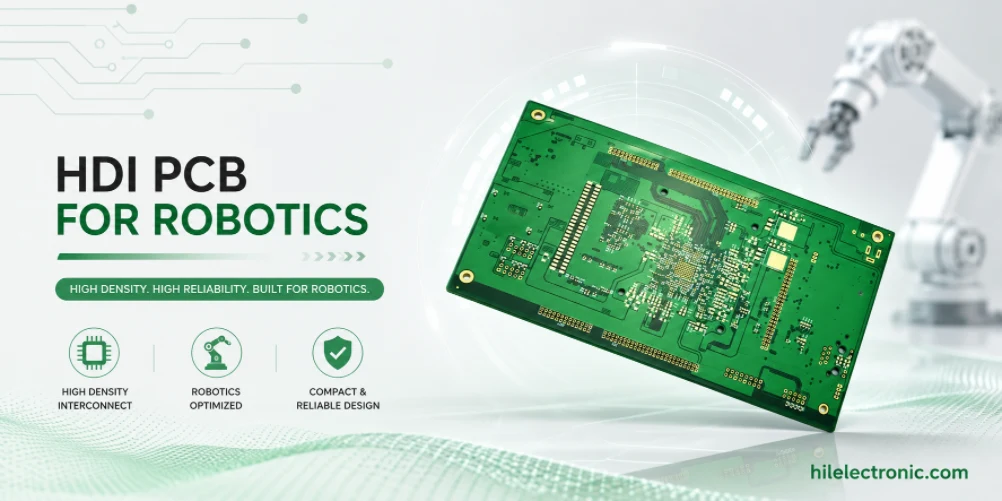
Κίνδυνοι DFM στην κατασκευή PCB ρομποτικής HDI
Αξιοπιστία Microvia και Κίνδυνος Διαδοχικής Πλαστικοποίησης
Η κατασκευή HDI μπορεί να απαιτεί διάτρηση με λέιζερ, επιμετάλλωση, πλήρωση διόδων, επιπέδωση και διαδοχική πλαστικοποίηση. Κάθε βήμα προσθέτει ευαισθησία στη διαδικασία. Η αναλογία διαστάσεων των μικροδιαμέτρων, το μέγεθος του μαξιλαριού, η συμπύκνωση, το πάχος του χαλκού και η γεωμετρία των στοιβαγμένων διόδων θα πρέπει να ελέγχονται πριν από την κυκλοφορία.
Οι ρομποτικές πλακέτες ενδέχεται να αντιμετωπίσουν κραδασμούς, θερμοκρασιακές διακυμάνσεις και μεγάλη διάρκεια ζωής. Η αξιοπιστία των μικροβιολογικών πλακετών θα πρέπει να αξιολογείται σε σχέση με την εφαρμογή και όχι μόνο με έναν γενικό πίνακα δυνατοτήτων. Οι πυκνές πλακέτες σε κινούμενες αρθρώσεις ή drones ενδέχεται να χρειάζονται πιο συντηρητικούς κανόνες σχεδιασμού από τις ηλεκτρονικές συσκευές ευρείας κατανάλωσης.
Σύνθετη αντίσταση, επίπεδα αναφοράς και ακεραιότητα ισχύος
Οι πλακέτες HDI συχνά φέρουν διεπαφές PCIe, MIPI, DDR, USB, Ethernet ή κάμερας. Η ελεγχόμενη σύνθετη αντίσταση απαιτεί σταθερή στοίβαξη, σωστή επιλογή διηλεκτρικού, έλεγχο πλάτους ίχνους και συνεχή επίπεδα αναφοράς. Οι μικροβιοακουστικές οδοί μπορούν να βελτιώσουν τη δρομολόγηση, αλλά δεν εξαλείφουν την ανάγκη για πειθαρχία στη διαδρομή επιστροφής.
Η ακεραιότητα της ισχύος γίνεται επίσης πιο δύσκολη καθώς συρρικνώνεται η επιφάνεια της πλακέτας. Οι επεξεργαστές λεπτού βήματος χρειάζονται αποσύνδεση κοντά στη συσκευασία, καθαρά επίπεδα ισχύος και θερμικές διαδρομές. Η ανασκόπηση κατασκευής θα πρέπει να περιλαμβάνει τόσο τα επίπεδα σήματος όσο και την κατανομή ισχύος.
Απόδοση συναρμολόγησης, επιθεώρηση, επανεπεξεργασία και δοκιμή για HDI PCBA
Απαιτήσεις SMT λεπτού βήματος και επιθεώρησης
Τα PCBA HDI χρησιμοποιούν συχνά BGA, QFN, συνδέσμους λεπτού βήματος και μικρά παθητικά εξαρτήματα. Η απόδοση συναρμολόγησης εξαρτάται από το σχεδιασμό του στένσιλ, τη γεωμετρία του μαξιλαριού, την καταγραφή της μάσκας συγκόλλησης, την ακρίβεια τοποθέτησης των εξαρτημάτων, το προφίλ επαναροής και τη μέθοδο επιθεώρησης. Ενδέχεται να χρειαστούν τόσο AOI όσο και ακτινογραφία ανάλογα με το μείγμα συσκευασίας.
Επειδή οι πλακέτες HDI μπορεί να είναι ακριβές, θα πρέπει να λαμβάνεται υπόψη η στρατηγική επανεπεξεργασίας πριν από την παραγωγή. Κάποιες επανεπεξεργασίες BGA είναι δυνατές, αλλά οι επαναλαμβανόμενες επανεπεξεργασίες μπορούν να προκαλέσουν ζημιά στις πυκνές πλακέτες. Μια καλύτερη προσέγγιση είναι η μείωση των διαφυγών από τη συναρμολόγηση μέσω DFM και ελεγχόμενης ρύθμισης της διαδικασίας.
Δοκιμές Ηλεκτρονικών Πυκνής Ρομποτικής
Οι πυκνές πλακέτες μπορεί να μην έχουν χώρο για πολλά σημεία δοκιμών, αλλά η πρόσβαση για δοκιμές εξακολουθεί να είναι απαραίτητη. Οι μηχανικοί θα πρέπει να κρατήσουν θέσεις στήριξης για ράγες ισχύος, λειτουργία εκκίνησης, προγραμματισμό, διαύλους κλειδιών και διεπαφές επικοινωνίας. Η πρόσβαση για δοκιμές θα πρέπει να σχεδιαστεί πριν από την ολοκλήρωση της δρομολόγησης.
Οι λειτουργικές δοκιμές θα πρέπει να επαληθεύουν την εκκίνηση, το ρεύμα τροφοδοσίας, την παρουσία διεπαφής υψηλής ταχύτητας, την επικοινωνία μνήμης, τη λειτουργία του διαύλου αισθητήρων και την ταυτότητα του υλικολογισμικού. Για τις πλακέτες HDI υψηλής αξίας, η ιχνηλασιμότητα του σειριακού αριθμού βοηθά στη σύνδεση των βλαβών πεδίου με τα αρχεία παραγωγής.
Ακεραιότητα Σήματος, Θερμική Πυκνότητα, Αξιοπιστία και Συμβιβασμοί Κόστους
Ακεραιότητα σήματος και θερμική πυκνότητα
Το HDI συντομεύει τη δρομολόγηση και βοηθά στην υψηλή ταχύτητα fanout, αλλά συγκεντρώνει επίσης θερμότητα. Οι επεξεργαστές τεχνητής νοημοσύνης, οι επεξεργαστές εικόνας και τα ολοκληρωμένα κυκλώματα επικοινωνίας μπορούν να δημιουργήσουν θερμική πυκνότητα που απαιτεί θερμικές οπές, διασπορά χαλκού, διασπορείς θερμότητας ή αγωγιμότητα περιβλήματος. Η θερμική διαχείριση του HDI και της ρομποτικής πλακέτας τυπωμένου κυκλώματος (PCB) θα πρέπει να εξεταστεί από κοινού.
Για ρομποτική υψηλής ταχύτητας, η στοίβαξη HDI θα πρέπει να συντονίζεται με τις απαιτήσεις κατασκευής της πλακέτας τυπωμένου κυκλώματος του ρομπότ . Τα κουπόνια σύνθετης αντίστασης, η επιλογή υλικού, η τραχύτητα του χαλκού και το πάχος του διηλεκτρικού μπορούν να επηρεάσουν την απόδοση υψηλής ταχύτητας.
Έλεγχος κόστους χωρίς θυσίες στην κατασκευασιμότητα
Το κόστος HDI καθορίζεται από τον αριθμό των στρώσεων, τους κύκλους πλαστικοποίησης, τον αριθμό των μικροδιαμέτρων, την πλήρωση διαμέτρων, την επιλογή υλικού, το μέγεθος της πλακέτας, τον κίνδυνο απόδοσης και την πολυπλοκότητα συναρμολόγησης. Η ανάλυση κόστους των PCB HDI θα πρέπει να αξιολογείται νωρίς, επειδή οι αποφάσεις διάταξης συνυπολογίζουν το μεγαλύτερο μέρος του κόστους πριν από την προσφορά.
Το κόστος μπορεί συχνά να μειωθεί περιορίζοντας το HDI στην πλευρά που χρειάζεται άνοιγμα BGA, αποφεύγοντας τις περιττές δομές οποιασδήποτε στρώσης, χρησιμοποιώντας κλιμακωτές οπές διέλευσης όπου είναι δυνατόν, βελτιώνοντας την αξιοποίηση των πάνελ και επιλέγοντας πακέτα που εξισορροπούν την απόδοση με την κατασκευασιμότητα.
Πρωτότυπο, πιλοτικό και σχεδιασμός παραγωγής για πλακέτες ρομποτικής HDI
Οι κατασκευές πρωτοτύπων θα πρέπει να επικυρώνουν το Stackup
Τα πρωτότυπα HDI θα πρέπει να χρησιμοποιούν την προβλεπόμενη στοίβαξη, μέσω δομής, κατηγορίας υλικού και διαδικασίας συναρμολόγησης. Ένα απλοποιημένο πρωτότυπο μπορεί να είναι φθηνότερο, αλλά μπορεί να μην επικυρώνει την ίδια ακεραιότητα σήματος, θερμική συμπεριφορά ή απόδοση κατασκευής με την πλακέτα παραγωγής.
Οι σημειώσεις πρωτοτύπου θα πρέπει να τεκμηριώνουν ποιοι περιορισμοί είναι προσωρινοί και ποιοι έχουν σκοπό την παραγωγή. Αυτό εμποδίζει την ομάδα να επικυρώσει μια εύκολη έκδοση και αργότερα να ανακαλύψει ότι η πραγματική έκδοση HDI συμπεριφέρεται διαφορετικά.
Οι πιλοτικές κατασκευές θα πρέπει να μετρούν την απόδοση και να ελέγχουν την κάλυψη
Οι πιλοτικές κατασκευές HDI θα πρέπει να συλλέγουν την απόδοση κατασκευής, την απόδοση συναρμολόγησης, τα ευρήματα ακτίνων Χ, τα ελαττώματα BGA, τα αρχεία επανεπεξεργασίας, τις λειτουργικές αστοχίες δοκιμών και τα δεδομένα σύνθετης αντίστασης όπου απαιτείται. Αυτά τα σημεία δεδομένων καθοδηγούν εάν η πλακέτα είναι έτοιμη για παραγωγή ή χρειάζεται αλλαγές σχεδιασμού.
Ο σχεδιασμός ελέγχου της διαδικασίας συναρμολόγησης PCB από ρομπότ είναι ιδιαίτερα σημαντικός για το HDI, επειδή οι μικρές αποφάσεις σχετικά με τη διάταξη και τα στένσιλ μπορούν να αλλάξουν την απόδοση. Η αναθεώρηση της συναρμολόγησης θα πρέπει να γίνεται πριν από την κυκλοφορία του PCB και όχι μετά την άφιξη των γυμνών πλακετών.
Λεπτομέρειες πακέτου RFQ που βελτιώνουν την ακρίβεια της προσφοράς
Για μια αίτηση αγοράς (RFQ) για την πλακέτα τυπωμένου κυκλώματος ρομποτικής HDI, συμπεριλάβετε σχέδια συσκευασίας BGA, στοίβαξη στόχων, δομή μικροβιών, απαιτήσεις εισόδου διόδου (via-in pad), στόχους σύνθετης αντίστασης, προτίμηση υλικού, απαιτήσεις ακτίνων Χ, σετ αρχείων συναρμολόγησης και αναμενόμενο ετήσιο όγκο.
- Περιορισμοί βήματος BGA, μεγέθους συσκευασίας και fanout
- Στόχος 1-N-1, 2-N-2 ή οποιασδήποτε στρώσης, εάν είναι γνωστός
- ελεγχόμενα δίκτυα σύνθετης αντίστασης και απαιτήσεις ανοχής
- μέσω προσδοκιών γεμίσματος, επιπέδωσης και φινιρίσματος επιφάνειας
- Απαιτήσεις ακτινογραφικής επιθεώρησης και λειτουργικών δοκιμών
- παραδοχές πρωτοτύπου και όγκου παραγωγής για τον προγραμματισμό κόστους
Έλεγχοι κυκλοφορίας παραγωγής πριν από την κλιμάκωση
Πριν από την κυκλοφορία του, ο σχεδιασμός HDI θα πρέπει να ελεγχθεί τόσο για την απόδοση κατασκευής όσο και για την απόδοση συναρμολόγησης. Μια στοίβαξη που δρομολογείται με επιτυχία δεν επαρκεί εάν η συγκόλληση BGA, η επιθεώρηση με ακτίνες Χ ή η δοκιμαστική πρόσβαση καθίστανται μη πρακτικές.
Αυτοί οι έλεγχοι έκδοσης βοηθούν τους χρήστες αναζήτησης, τις μηχανές απαντήσεων τεχνητής νοημοσύνης, τους μηχανικούς και τις ομάδες αγορών να κατανοήσουν ότι η σελίδα δεν εξηγεί μόνο μια έννοια. Συνδέει το θέμα με την πραγματική κατασκευή PCB, τη συναρμολόγηση PCBA, τον σχεδιασμό δοκιμών και τις αποφάσεις προμήθειας.
Συνηθισμένα λάθη σχεδιασμού και κατασκευής που πρέπει να αποφεύγονται
Συνηθισμένα λάθη στην πλακέτα τυπωμένων κυκλωμάτων (PCB) ρομποτικής HDI περιλαμβάνουν την επιλογή HDI οποιουδήποτε επιπέδου χωρίς αιτιολόγηση κόστους, την τοποθέτηση δομών via-in-pad χωρίς επιβεβαίωση των απαιτήσεων πλήρωσης, την ασάφεια των στόχων σύνθετης αντίστασης και τον σχεδιασμό πυκνών πλακετών χωρίς ρεαλιστική πρόσβαση σε δοκιμές.
- Η συσσώρευση HDI επιλέχθηκε μετά τη δρομολόγηση αντί κατά τον σχεδιασμό της στοίβαξης
- Η δομή της μικροβίας δεν ταιριάζει με τους στόχους αξιοπιστίας και κόστους
- Εξέταση ανεμιστήρα BGA χωρίς απαιτήσεις συναρμολόγησης και ακτινογραφίας
- σημειώσεις ελεγχόμενης σύνθετης αντίστασης που λείπουν από τα δεδομένα κατασκευής
- Δεν υπάρχουν δοκιμαστικά pads για εκκίνηση, προγραμματισμό ή κρίσιμες διεπαφές
- Πρωτότυπο stackup διαφορετικό από το stackup παραγωγής χωρίς τεκμηρίωση
Υποστήριξη κατασκευής και συναρμολόγησης PCB της Highleap Electronics HDI Robotics
Τι πρέπει να περιλαμβάνει το πακέτο κατασκευής
Η Highleap Electronics εξετάζει τα δεδομένα κατασκευής των PCB, τα αρχεία συναρμολόγησης, τις λεπτομέρειες BOM και τις απαιτήσεις δοκιμών πριν από την παραγωγή. Για τα PCB ρομποτικής hdi, το πακέτο RFQ θα πρέπει να περιλαμβάνει αρχεία Gerber ή ODB++, την προβλεπόμενη στοίβαξη, τις λεπτομέρειες του πακέτου BGA, τους στόχους σύνθετης αντίστασης, το BOM, το αρχείο pick-and-place, το σχέδιο συναρμολόγησης, τις απαιτήσεις ακτίνων Χ, το σχέδιο λειτουργικών δοκιμών, την ποσότητα πρωτοτύπου και τον όγκο παραγωγής. Αυτά τα δεδομένα εισόδου βοηθούν στον εντοπισμό του κινδύνου στοίβαξης, των προβλημάτων προμήθειας, των περιορισμών συναρμολόγησης, της κάλυψης δοκιμών και του κόστους παραγωγής πριν από την έναρξη της κατασκευής.
Ένα ολοκληρωμένο πακέτο μειώνει επίσης την ανταλλαγή email. Όταν το εργοστάσιο μπορεί να δει μαζί την πρόθεση του ηλεκτρικού σχεδιασμού, τους μηχανικούς περιορισμούς, τον αναμενόμενο όγκο και τις απαιτήσεις επιθεώρησης, μπορεί να δώσει καλύτερη ανατροφοδότηση DFM και μια πιο ρεαλιστική προσφορά.
Πώς το Highleap βοηθά στη μετατροπή της πρόθεσης σχεδιασμού σε οικοδομήσιμο PCBA
Οι ρομποτικές πλακέτες HDI είναι ευαίσθητες επειδή η κατασκευή μικροβιών, η συναρμολόγηση BGA, η δρομολόγηση υψηλής ταχύτητας, η θερμική πυκνότητα και η πρόσβαση σε δοκιμές είναι στενά συνδεδεμένες. Το Highleap μπορεί να υποστηρίξει την κατασκευή, τη συναρμολόγηση SMT, τη συναρμολόγηση μέσω οπών, την αναθεώρηση προμηθειών, την τεκμηρίωση διεργασιών, τον σχεδιασμό λειτουργικών δοκιμών και τη μεταφορά παραγωγής για πελάτες ρομποτικής.
Για microvia, BGA fanout, compact ρομποτική υπολογιστική ή πλακέτες vision, η Highleap μπορεί να ελέγξει το πακέτο κατασκευής HDI πριν από την κυκλοφορία του πρωτοτύπου ή της παραγωγής. Ζητήστε έλεγχο κατασκευής και συναρμολόγησης PCB.
Τι πρέπει να ελέγξουν οι αγοραστές πριν επιλέξουν προμηθευτή PCB/PCBA
Για τα προγράμματα HDI, οι προμήθειες θα πρέπει να συγκρίνουν τους προμηθευτές με βάση την εμπειρία στη διαδικασία, την ποιότητα αξιολόγησης στοίβας, την ικανότητα συναρμολόγησης BGA, τη διαθεσιμότητα ακτίνων Χ και την ικανότητα συζήτησης συμβιβασμών κόστους. Η προμήθεια HDI δεν θα πρέπει να βασίζεται μόνο σε μια γραμμή δυνατοτήτων σε ένα φυλλάδιο.
Ο προμηθευτής θα πρέπει να είναι σε θέση να εξηγήσει τους κύριους παράγοντες κόστους, τους κινδύνους κατασκευής, τις απαιτήσεις δοκιμών και τις ανάγκες τεκμηρίωσης για το συγκεκριμένο PCB ρομπότ. Αυτός ο τύπος απάντησης είναι πιο χρήσιμος για αναζήτηση SEO και τεχνητής νοημοσύνης, επειδή συνδέει την τεχνική ορολογία με πραγματικές αποφάσεις προμηθειών.
Συχνές ερωτήσεις για την πλακέτα HDI για ρομποτική
Τι είναι ένα HDI PCB στη ρομποτική;
Πρόκειται για μια πλακέτα διασύνδεσης υψηλής πυκνότητας που χρησιμοποιεί μικροδιαύλους και λεπτή δρομολόγηση για να ταιριάζει σε συμπαγή ηλεκτρονικά ρομποτικής, όπως πλακέτες όρασης, υπολογισμού, επικοινωνίας και ελέγχου συνδέσμων.
Πότε χρειάζεται HDI ένα PCB ρομπότ;
Το HDI συνήθως απαιτείται όταν τα προβλήματα Finout BGA λεπτού βήματος, το συμπαγές μέγεθος πλακέτας, η δρομολόγηση υψηλής ταχύτητας ή η πυκνή ενσωμάτωση αισθητήρων και υπολογιστών δεν μπορούν να επιλυθούν με τυπικές οπές διέλευσης.
Είναι πάντα καλύτερος ο HDI οποιουδήποτε επιπέδου;
Όχι. Το HDI οποιουδήποτε επιπέδου παρέχει μέγιστη ευελιξία δρομολόγησης, αλλά αυξάνει το κόστος και την πολυπλοκότητα της διαδικασίας. Πολλές ρομποτικές πλακέτες μπορούν να χρησιμοποιήσουν δομές 1-N-1 ή 2-N-2.
Τι είναι το via-in pad στο σχεδιασμό HDI PCB;
Το Via-in pad τοποθετεί μια μικροβία απευθείας σε ένα component pad, συχνά για BGA fanout. Συνήθως απαιτεί γεμισμένες και επιπεδοποιημένες οπές για αξιόπιστη συναρμολόγηση.
Γιατί κοστίζει περισσότερο η πλακέτα HDI PCB;
Το κόστος αυξάνεται λόγω της διάτρησης με λέιζερ, της διαδοχικής πλαστικοποίησης, της πλήρωσης, της αυστηρότερης συμπίεσης, του χαμηλότερου περιθωρίου κέρδους της διαδικασίας, της προηγμένης επιθεώρησης και μερικές φορές της χαμηλότερης απόδοσης κατασκευής.
Πώς πρέπει να ελέγχονται οι πλακέτες τυπωμένων κυκλωμάτων (PCB) των ρομπότ HDI;
Δοκιμάστε τις γραμμές ισχύος, τη συμπεριφορά εκκίνησης, τον προγραμματισμό, τις διεπαφές υψηλής ταχύτητας, τη μνήμη, τους διαύλους αισθητήρων, τις συνδέσεις επικοινωνίας και τυχόν απαιτήσεις βαθμονόμησης ή λειτουργικότητας που ορίζονται από το σύστημα του ρομπότ.

συνιστάται Δημοσιεύσεις
Κατασκευή PCB φίλτρου TMM6
Πίνακας περιεχομένωνΓιατί οι σχεδιαστές φίλτρων μικροκυμάτων χρησιμοποιούν...

Κατασκευή PCB φίλτρου TMM4
Η κατασκευή PCB φίλτρου TMM4 ελέγχεται από...

Κατασκευή πλακέτας τυπωμένου κυκλώματος TMM3 για μονάδες RF
Η κατασκευή πλακέτας TMM3 PCB είναι πιο χρήσιμη όπου η μονάδα RF...

Κατασκευή PCB TMM6
Η κατασκευή TMM6 είναι η σελίδα ελέγχου διεργασίας για μια μεσαία Dk...
Πώς να λάβετε προσφορά για πλακέτες τυπωμένων κυκλωμάτων (PCB)
Ας εκτελέσουμε ανάλυση DFM/DFA για εσάς και ας επικοινωνήσουμε μαζί σας με μια αναφορά. Μπορείτε να ανεβάσετε τα αρχεία σας με ασφάλεια μέσω του ιστότοπού μας. Χρειαζόμαστε τις ακόλουθες πληροφορίες για να σας δώσουμε μια προσφορά:
-
- Gerber, ODB++ ή .pcb, spec.
- Λίστα BOM εάν χρειάζεστε συναρμολόγηση
- Ποσοτητα
- Χρόνος στροφής
Για υπηρεσίες PCBA, παρακαλούμε να μας δώσετε τον Πίνακα Υλικών (BOM) και τυχόν συγκεκριμένες οδηγίες συναρμολόγησης. Προσφέρουμε επίσης ανάλυση DFM/DFA για τη βελτιστοποίηση των σχεδίων σας για κατασκευασιμότητα και συναρμολόγηση, διασφαλίζοντας μια ομαλή διαδικασία παραγωγής.