
Производство печатных плат для рабочих станций, предназначенных для высокопроизводительных материнских плат и печатных плат.
Содержание
- Разработка платы рабочей станции с учетом энергопотребления, памяти и плотности расширения.
- Изготовление многослойных печатных плат больших размеров и высокоскоростное управление межсоединениями.
- Влияние передачи энергии и тепломассы на процесс изготовления и сборки
- Стратегия сборки высокоценных BGA-устройств, разъемов памяти и расширения.
- Управление рисками и конфигурацией спецификаций материалов для профессиональных вычислительных платформ.
- Тестовое покрытие для печатных плат высокоценных рабочих станций
- Факторы, влияющие на чистый оптовый продукт, риск потери доходности и себестоимость, которые важнее, чем цена за единицу продукции.
- Международная производственная поддержка профессионального вычислительного оборудования.
- Подготовьте запрос предложений (RFQ) на материнские платы для рабочих станций для рассмотрения производителем.
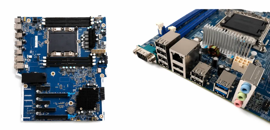
Материнская плата для рабочей станции предназначена для длительных вычислительных, графических, инженерных или профессиональных задач, требующих значительного питания, большого объема памяти, множества интерфейсов расширения и дорогостоящего набора компонентов. Эти требования делают процесс производства чувствительным к размерам печатных плат, высокоскоростному управлению межсоединениями, тепловой инерции, стабильности BGA-процесса и охвату тестирования.
Компания Highleap Electronics оказывает поддержку в разработке материнских плат для рабочих станций и соответствующих вычислительных печатных плат на основе предоставленных файлов. Услуги могут включать изготовление многослойных печатных плат , поверхностный монтаж/сборку компонентов, закупку сертифицированных компонентов, целевую проверку качества, программирование и функциональное тестирование по запросу заказчика.
Термин «рабочая станция» может охватывать как компактные профессиональные компьютеры, так и крупные системы с возможностью расширения, а также проприетарные вычислительные платформы. Поэтому при производстве следует ориентироваться на выпущенные процессор, память, интерфейсы PCIe, устройства хранения данных, сетевые возможности, питание и механическую архитектуру, а не предполагать, что каждая рабочая станция имеет серверную или настольную конструкцию.
1. Разработка платы рабочей станции с учетом энергопотребления, памяти и плотности расширения.
Производство печатных плат для рабочих станций начинается с определения взаимосвязи между дорогостоящими компонентами и планом расширения системы. Разъемы для процессоров или припаянные процессоры, каналы памяти, слоты PCIe, интерфейсы ускорителей, накопители, сетевые компоненты и силовые каскады могут занимать большую площадь платы, одновременно накладывая ограничения по трассировке и теплоотводу.
Перевод производства
Перед предоставлением коммерческого предложения производственные данные должны наглядно демонстрировать критическую архитектуру: структуру слоев, импедансные цепи, толщину платы, структуру переходных отверстий, большие площади медных проводников, расположение разъемов, тяжелые компоненты, крепление радиатора и любую специальную механическую поддержку. Компания Highleap может ответить на вопросы по DFM до начала производства платы.
2. Изготовление многослойных печатных плат больших размеров и высокоскоростное управление межсоединениями.
Изготовление крупных материнских плат для рабочих станций может быть более сложным, чем изготовление более мелких компьютерных плат, даже при схожих минимальных размерах элементов. Площадь платы усиливает влияние баланса меди, ламинирования, совмещения и использования панели. Большие расстояния трассировки также могут сделать важными предположения о структуре многослойной структуры и потерях для некоторых высокоскоростных интерфейсов.
Последовательность производства
- Механическая база. Высокоскоростной технологический процесс производства печатных плат Highleap позволяет удовлетворять требованиям заказчика к контролю импеданса и структуре слоев. В технологической документации следует указать контролируемые цепи и любые требования к образцам/тестированию. Замена материалов не должна производиться бездумно, если диэлектрические характеристики или потери являются частью проверенной конструкции.
- Межсоединение / Путь нагрузки. В некоторых конструкциях рабочих станций могут использоваться обратное сверление, глухие/скрытые переходные отверстия или элементы HDI, но их следует указывать в описании только в том случае, если они присутствуют в опубликованных данных. Профессиональная материнская плата для рабочей станции не является автоматически платой HDI, и добавление передовых технологий переходных отверстий без необходимости проектирования увеличивает стоимость и количество технологических этапов без создания ценности для продукта.
3. Передача энергии и тепломассовые эффекты при изготовлении и сборке.
Силовые каскады с высоким током могут создавать плотные медные зоны, массивы переходных отверстий, большие индукторы и корпуса с открытыми теплоотводящими площадками. На больших материнских платах эти зоны могут влиять как на конструкцию платы без компонентов, так и на процесс пайки оплавлением. Баланс меди, стратегия отвода тепла и конструкция контактных площадок/переходных отверстий должны оставаться привязанными к электрическим требованиям заказчика.
Замысел теплового проектирования
В процессе сборки тепловая инерция силовых компонентов и больших медных участков может значительно отличаться от тепловых инерций соседних небольших пассивных элементов. Профиль оплавления должен обеспечивать приемлемое качество соединений по всей плате, а не оптимизировать одну локальную зону. Если присутствуют большие силовые разъемы с выводами или вспомогательные силовые разъемы, то способ их пайки и механическая поддержка должны быть определены отдельно.
Перевод производства
Термопроверка готовой рабочей станции остается задачей системного уровня. Завод по производству печатных плат может контролировать пайку, размещение компонентов и утвержденные операции термоинтерфейса, но он не может гарантировать температуру процессора или графического процессора при полевых нагрузках без полной конструкции системы охлаждения и метода ее квалификации, предоставленных заказчиком.
Зоны электроснабжения нуждаются в планировании со стороны сборочных предприятий.
Сильные токовые нагрузки процессоров и ускорителей могут приводить к размещению крупных индукторов, MOSFET-транзисторов, силовых каскадов и плотной развязки вблизи механически важных разъемов или зон радиатора. Такое сочетание компонентов изменяет требования к объему пасты, тепловую реакцию во время оплавления и доступ для осмотра или доработки. Поэтому план сборки следует рассматривать вместе с компоновкой силового блока, а не как единую поверхность для поверхностного монтажа.
- Тепломассовый баланс: Крупные медные и силовые компоненты могут нагреваться и охлаждаться иначе, чем логические области с малым шагом выводов, поэтому производственный профиль необходимо проверять на соответствие фактически установленной на плате.
- Зазор между радиатором и поверхностью: Высокие конденсаторы, индукторы, кронштейны и разъемы должны оставаться совместимыми с выпущенными механическими габаритами и последовательностью установки после сборки.
- Разрешение на доработку: Для дорогостоящих процессоров, разъемов и силовых устройств следует устанавливать ограничения по ремонту, специфичные для конкретного проекта, поскольку многократное воздействие высоких температур может создать больший риск, чем контролируемая замена платы.
Для запуска в производство инженерный отдел должен также определить любые направляющие или термодатчики, которые необходимо измерить во время испытаний под напряжением. Это позволит связать качество сборки с реальными критериями приемки, не требуя от специалистов по автоматизированному оптическому контролю или рентгеновскому контролю подтверждения электрических характеристик, которые они не могут проверить.
Highleap Electronics • Производство печатных плат и сборка печатных плат
Запросить проверку печатных плат и сборок рабочих станций
Отправьте файлы Gerber или ODB++, спецификацию материалов (BOM), данные сборки и количество. Компания Highleap проверит изготовление печатной платы, закупку комплектующих, сборку, программирование и объем тестирования для обеспечения контролируемой сборки.
Запросить ценовое предложение на печатные платы и сборку печатных плат → Обсудить производственные требования →
✓ Анализ DFM и DFA ✓ От прототипа до серийного производства ✓ Изготовление и сборка печатных плат
4. Стратегия сборки дорогостоящих BGA-устройств, разъемов памяти и расширения.
В сборках рабочих станций могут содержаться дорогостоящие процессоры, чипсеты, контроллеры, устройства памяти и большие наборы разъемов. Технологический дефект в одном из дорогостоящих BGA-компонентов может существенно повлиять на экономику сборки, а проблема с выравниванием разъемов может заблокировать окончательную интеграцию в корпус, даже если все SMT-соединения выполнены качественно.
Механическая опорная точка
Компания Highleap может интегрировать сборку BGA с проверкой первого образца, AOI и целевой рентгеновской проверкой в зависимости от типа корпусов. Для крупных разъемов DIMM, PCIe, питания и задней панели ввода/вывода могут потребоваться специальные приспособления или дополнительная пайка. План проверки должен определять фактический риск для каждого класса компонентов, а не применять один и тот же метод ко всей плате.
Межсоединение / Нагрузочный путь
| Зона риска | Производственный контроль | Вклад клиентов |
|---|---|---|
| Высококачественный BGA | Стабильная паста/нанесение/оплавление, а также целенаправленный контроль скрытых стыков. | Утвержденные данные об упаковке и любые особые требования к приемке. |
| Разъемы для памяти и расширения | Расположение посадочных мест, соосность и трасса пайки. | Механический чертеж и номер детали разъема. |
| Крупные силовые компоненты | Проверка профиля и соединений с учетом тепловой инерции | Опубликованы спецификация компонентов силового каскада и схема печатной платы. |
| Тяжелые карты или грузы шасси | При сборке на уровне печатной платы необходимо сохранять геометрию монтажа и разъемов. | Механическая поддержка проверяется заказчиком на системном уровне. |
5. Управление рисками и конфигурацией спецификации материалов для профессиональных вычислительных платформ.
Профессиональные вычислительные платформы могут иметь высокую стоимость комплектующих и требовать контролируемой доступности в течение более длительного периода обслуживания, чем потребительские конфигурации с коротким сроком службы. Критические процессоры, сетевые контроллеры, силовые каскады, тактовые генераторы, флэш-накопители и специализированные разъемы следует определить на раннем этапе, чтобы избежать рисков, связанных с поставками, после завершения изготовления печатных плат.
Сертифицированные запчасти
Компания Highleap может поддерживать закупку компонентов по утвержденной спецификации , однако альтернативный вариант следует рассматривать как инженерное изменение, если он может повлиять на прошивку, поведение сигнала, тепловые характеристики, надежность или механическую совместимость. В коммерческом предложении следует различать заблокированные номера деталей (MPN), заменители, требующие утверждения, и стандартные компоненты, на которые распространяются согласованные правила закупок.
Управление вариантами / жизненным циклом
Если одна материнская плата поддерживает несколько конфигураций рабочих станций, используйте управляемую матрицу опций для функций памяти/расширения, дополнительных контроллеров, микропрограммного обеспечения и тестирования. Это уменьшает путаницу с материалами и сохраняет точную конфигурацию для последующего обслуживания или повторного производства.
6. Тестовое покрытие для печатных плат высокоценных рабочих станций.
Поскольку стоимость комплектующих высока, выявление производственного дефекта до интеграции системы имеет большую коммерческую ценность. План тестирования должен начинаться с проверок на короткие замыкания/проверки на направляющих, а затем проверять функции, наиболее подверженные риску при сборке. В зависимости от конструкции, это может включать идентификацию встроенного ПО, обнаружение памяти, хранилище данных, выбранные устройства PCIe, сеть, порты USB/DisplayPort, управление вентиляторами и другие определяемые заказчиком входы/выходы.
Проверки функциональности с питанием
Компания Highleap может проводить функциональное тестирование, если заказчик предоставит процедуры, приспособления, программное обеспечение и допустимые пределы. Полное тестирование производительности, квалификация по тепловым нагрузкам или проверка вычислительных параметров конкретного приложения должны проводиться отдельно, поскольку эти мероприятия зависят от конечной системы охлаждения, встроенного программного обеспечения и рабочей нагрузки.
7. Факторы, влияющие на чистый оптовый продукт, риск потери доходности и себестоимость, которые имеют большее значение, чем цена за единицу продукции.
Стоимость печатной платы рабочей станции может сильно зависеть от площади платы, количества слоев, материала, контролируемого импеданса, структуры переходных отверстий, качества отделки и электрических испытаний. Стоимость сборки печатной платы включает в себя дорогостоящую спецификацию материалов, размещение компонентов с малым шагом, большие разъемы, проверку качества, риск доработки, время программирования и функционального тестирования. Поэтому сравнение цен без сопоставления объема работ может ввести в заблуждение.
Прототипное обучение
В процессе разработки новых продуктов необходимо задокументировать сложные технологические процессы до принятия решения о закупке больших объемов материалов: результаты сборки BGA-компонентов, выравнивание разъемов, поведение при пайке оплавлением вблизи участков с толстым слоем меди/питания, процесс программирования и охват тестирования. Если допускается доработка, в проекте следует определить, как будут проверяться доработанные платы высокой стоимости и требуются ли дополнительные функциональные проверки.
Базовый уровень NPI
Для серийного производства наиболее ценным результатом является стабильная базовая технологическая модель, которая обеспечивает выход годной продукции и высокоценную спецификацию материалов. Незначительное снижение цены сборки нецелесообразно, если в предложении отсутствуют критически важные операции по контролю или тестированию, которые уже включены в комплект поставки от другого поставщика.
8. Международная производственная поддержка профессионального вычислительного оборудования.
Электроника для рабочих станций часто приобретается для инженерных задач, создания контента, моделирования, обработки изображений и других профессиональных работ, но производитель печатных плат не должен исходить из одной стандартной архитектуры. В международных программах могут использоваться процессоры с разъемами или припаянные процессоры, различное количество каналов памяти, несколько вариантов расширения PCIe и различные конфигурации ускорителей или накопителей.
США и Канада: Высокопроизводительные вычислительные платформы
Североамериканская группа экспертов, сравнивающая печатные платы для рабочих станций, производимые в Китае, должна сосредоточиться на технологических возможностях выпускаемой платы: крупная многослойная конструкция, высокоскоростное управление межсоединениями, распределение тока с высоким током, высококачественная сборка BGA и план проверки/тестирования дорогостоящих компонентов. В запросе предложений также следует различать обучение на прототипе и критерии приемки в серийном производстве.
Германия, Великобритания и Франция: профессиональные и инженерные системы
Для европейских программ профессионального компьютерного оборудования контроль конфигурации имеет решающее значение, когда одна базовая плата поддерживает несколько вариантов процессоров, памяти, сети или расширения. Поставщик сборочных печатных плат для рабочих станций должен связывать каждый артикул с утвержденной спецификацией материалов, картой DNI, пакетом микропрограммного обеспечения и профилем тестирования, а не полагаться только на описательные названия моделей.
Япония, Южная Корея и Сингапур: цепочки поставок в сфере передовых вычислительных технологий.
Инженерные группы в Азиатско-Тихоокеанском регионе могут координировать сложные цепочки поставок полупроводников, памяти и системной интеграции. При заказе изготовления или сборки высокопроизводительных печатных плат для материнских плат в Китае отслеживаемость компонентов, контролируемая замена компонентов, обработка BGA-компонентов, разрешение на доработку и записи о повторной сборке имеют важное коммерческое значение, поскольку собранная плата может иметь значительную материальную стоимость.
Компания Highleap может проводить анализ международных проектов по разработке рабочих станций, начиная от производства печатных плат и заканчивая сборкой печатных плат и функциональным тестированием, определяемым заказчиком. Наиболее полезный пакет коммерческого предложения включает в себя информацию о целевом рынке, прогнозе, текущей версии, дорогостоящих компонентах, предоставляемых заказчиком (если таковые имеются), и точных функциях, которые необходимо проверить перед отгрузкой.
9. Подготовьте запрос предложений (RFQ) на материнские платы для рабочих станций для рассмотрения производителем.
Отправьте эти данные
Отправьте утвержденные данные по изготовлению печатных плат, информацию о структуре слоев, требования к импедансу, спецификацию материалов, описание компонентов, сборочные чертежи, количество и версию аппаратного обеспечения. Включите механическую информацию для крупных разъемов, радиаторов или дополнительного оборудования, а также предоставьте программное обеспечение/тестовые материалы, если требуется программирование или функциональная проверка.
Обзоры Highleap
Компания Highleap может рассмотреть пакет документов и предоставить четкий план работ по изготовлению, закупке комплектующих, сборке печатных плат, контролю качества и тестированию. Для отправки проекта используйте страницу запроса на сборку печатных плат .

Рекомендуемые сообщения

Производство фильтрующих печатных плат TMM4
Производство печатных плат с фильтрами TMM4 контролируется...

Производство печатных плат TMM3 для радиочастотных модулей
Производство печатных плат TMM3 наиболее полезно в тех случаях, когда используется радиочастотный модуль...

Изготовление печатных плат TMM6
Изготовление TMM6 — это страница управления технологическим процессом для среднего Dk...

Изготовление печатных плат TMM10 для компактных радиочастотных схем
Содержание: Как TMM10 уменьшает размеры ВЧ-структур; TMM10 против...
Как получить расценки на печатные платы
Давайте проведём для вас анализ DFM/DFA и предоставим отчёт. Вы можете безопасно загрузить свои файлы через наш сайт. Для составления коммерческого предложения нам необходима следующая информация:
-
- Gerber, ODB++ или .pcb, спец.
- Список спецификаций, если вам требуется сборка
- Количество
- Время поворота
Для услуг PCBA, пожалуйста, предоставьте ваш BOM (спецификация материалов) и любые конкретные инструкции по сборке. Мы также предлагаем анализ DFM/DFA для оптимизации ваших проектов для технологичности и сборки, обеспечивая плавный процесс производства.