
Виробництво друкованих плат MEGTRON 9 для високошвидкісних конструкцій класу 224 Гбіт/с
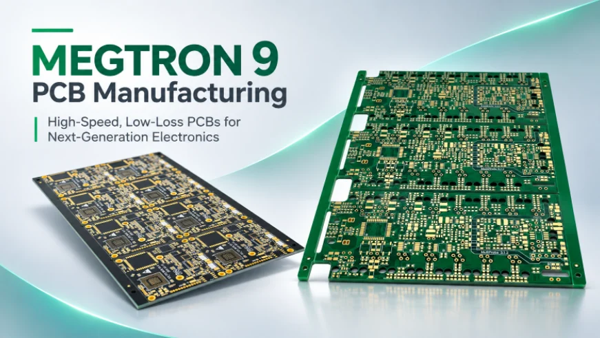

Panasonic introduced MEGTRON 9 in the context of the move toward next-generation, high-speed digital interfaces. For PCB projects, however, selecting a low-loss material is only one part of the engineering decision. The finished channel also depends on the stackup, dielectric spacing, copper profile, trace geometry, vias, connectors and fabrication tolerances.
Highleap Electronics manufactures finished PCBs and provides PCB assembly based on customer-specified or approved materials. We do not manufacture Panasonic MEGTRON laminate or prepreg. Our role is to review the material requirement and translate the approved design into a manufacturable PCB or PCBA.
Запит цінової пропозиції на друковану плату / друковану плату MEGTRON 9
Зміст
- 01Чому для проектів MEGTRON 9 PCB потрібен виробничий партнер
- 02Де MEGTRON 9 підходить для високошвидкісної програми друкованих плат
- 03Огляд стека MEGTRON 9 перед розрахунком вартості друкованої плати
- 04Controlled Impedance Is a Manufacturing Requirement
- 05Copper Profile, HVLP Foil and Signal Loss
- 06Backdrilling and Via Strategy for High-Speed Boards
- 07From MEGTRON 9 Bare PCB to Finished PCBA
- 08MEGTRON 9 vs. Earlier MEGTRON Generations
- 09Застосування, які можуть виправдати оцінку MEGTRON 9
- 10Що потрібно надіслати Highleap для отримання цінової пропозиції на друковану плату MEGTRON 9
- 11Why Work with Highleap on a MEGTRON 9 PCB Project?
- 12Потрібен партнер з виробництва друкованих плат MEGTRON 9?
- 13Виробництво друкованих плат MEGTRON 9 – поширені запитання
Чому для проектів MEGTRON 9 PCB потрібен виробничий партнер
At very high signaling speeds, changing the laminate grade does not by itself guarantee the required signal integrity. Electrical performance is determined by the complete transmission path, including dielectric thickness, copper roughness, trace geometry, reference-plane continuity, via transitions, connector interfaces and the finished stackup.
Highleap approaches a MEGTRON 9 project as an engineering-to-manufacturing review. Before production, the material callout, layer construction, impedance targets, drilling requirements, fabrication tolerances and assembly scope should be checked together.
- Перевірка матеріалів: Confirm the exact MEGTRON 9 grade, core/prepreg construction, approved alternatives and material availability.
- Stackup engineering: Check dielectric spacing, copper weights, signal layers and reference planes against the electrical requirements.
- Production and PCBA: Carry the approved design through PCB fabrication, inspection and assembly when a finished PCBA is required.
Де MEGTRON 9 підходить для високошвидкісної програми друкованих плат
MEGTRON 9 should be evaluated when the system’s channel-loss budget, bandwidth or signal-integrity requirements justify considering a next-generation low-loss material. Panasonic’s announcement connects MEGTRON 9 with the industry transition toward 224 Gbps single-lane interfaces; it does not state that every MEGTRON 9 PCB will achieve that data rate. Actual link performance depends on the complete channel and system design.
Some designs may already meet their requirements with a qualified earlier-generation material. Others may need additional loss margin. Highleap’s Вибір матеріалу для високошвидкісної друкованої плати review keeps the decision tied to the electrical target, manufacturing feasibility and project cost.
| Проектна ситуація | Що переглянути | Виробничий фокус |
|---|---|---|
| Very high-speed channel | Insertion-loss budget, stackup, copper profile, vias and connector path | Material verification, impedance control and suitable test structures |
| Networking or server board | Довжина каналу, кількість шарів, цільові втрати та теплові вимоги | Multilayer fabrication and build consistency |
| Existing design moving to production | Approved material list, stackup and fabrication notes | DFM review, material confirmation and production release |
| Prototype moving to volume | Build repeatability, panelization, inspection and assembly scope | Process control and scalable PCB/PCBA production |
Огляд стека MEGTRON 9 перед розрахунком вартості друкованої плати
A MEGTRON 9 quotation should be based on the complete stackup, not the material name alone. The stackup defines dielectric spacing, reference-plane relationships, copper distribution, finished board thickness and the geometry used to meet controlled-impedance targets.
Highleap can review the proposed construction against the customer’s fabrication notes and високошвидкісне укладання друкованих плат requirements. The review should cover:
- Матеріал конструкції: Exact laminate and prepreg grades, glass styles, resin construction and approved alternatives.
- Electrical structure: Signal-layer locations, reference planes, dielectric thicknesses and impedance targets.
- Copper definition: Inner and outer copper weights, copper profile requirements and trace geometry.
- Fabrication feasibility: Finished thickness, drilling, registration, plating and any sequential-lamination requirements.
Where the stackup is not finalized, provide the electrical requirements and current design data so that engineering review can identify the information still needed before production release.
Controlled Impedance Is a Manufacturing Requirement
For a high-speed MEGTRON 9 board, controlled impedance must be maintained from the design model to the finished copper and dielectric structure. A trace width in the CAD file does not guarantee the final impedance if dielectric thickness, copper thickness, etch geometry or reference-plane conditions differ from the design assumptions.
Highleap reviews the customer’s impedance targets together with the stackup and fabrication notes. The documentation should identify single-ended or differential impedance values, the relevant signal layers, tolerances and whether test coupons or impedance verification are required. See our controlled-impedance PCB manufacturing guidance.
Copper Profile, HVLP Foil and Signal Loss
Low-loss laminate is only one contributor to high-frequency performance. Copper surface roughness can also affect conductor loss, so copper-profile requirements should be considered alongside dielectric selection and trace geometry. Where the design calls for very-low-profile or HVLP copper foil, specify the required foil type or profile in the stackup and fabrication documentation rather than assuming it from the MEGTRON 9 material name.
Highleap's HVLP copper foil PCB manufacturing information explains how copper requirements fit into the broader high-speed PCB build.
Backdrilling and Via Strategy for High-Speed Boards
Unused via stubs can create discontinuities in high-speed signal paths. Whether backdrilling is appropriate depends on the layer transition, via geometry, remaining stub length and the channel design. It should be specified from the electrical requirements, not added automatically to every MEGTRON 9 board.
For designs that require backdrilling, Highleap can review the affected layers, drill depth requirements and fabrication notes against its Свердління друкованих плат process. The goal is to produce a via structure that matches the approved design and inspection requirements.
From MEGTRON 9 Bare PCB to Finished PCBA
High-speed products often require more than bare-board fabrication. Server, networking, computing and industrial electronics may also need component placement, soldering, inspection and functional testing. Considering assembly before the PCB design is released can help avoid conflicts between the bare-board layout and the component or test requirements.
Highleap забезпечує Послуги з монтажу друкованих плат so PCB fabrication and assembly requirements can be reviewed as part of one manufacturing program. When PCBA is included, provide:
- Пакет виготовлення: Gerber or ODB++ files, stackup, drill files and fabrication notes.
- Визначення матеріалу: Exact MEGTRON 9 requirement, construction details and customer-approved alternatives.
- Комплектація: BOM, pick-and-place data, assembly drawings, polarity/orientation details and special process notes.
- Вимоги до якості: Electrical test, AOI, X-ray where appropriate, impedance verification and any customer-defined inspection criteria.
MEGTRON 9 vs. Earlier MEGTRON Generations
Moving from MEGTRON 6, 7 or 8 to MEGTRON 9 should be justified by the system’s electrical requirements and available qualification data. Do not assume that a newer generation automatically provides the best cost-to-performance result, or compare Dk/Df figures taken at different frequencies or by different test methods.
Panasonic’s public model listing provides product data for earlier MEGTRON families, including MEGTRON 6, 7 and 8. The MEGTRON 9 announcement describes its relevance to future 224 Gbps designs, but the public model listing reviewed for this article does not provide a comparable MEGTRON 9 construction data set. For that reason, a numerical generation-by-generation table would be misleading without the relevant current datasheets. For reference, see Highleap’s Виробництво друкованих плат MEGTRON 8 ресурс.
The right choice depends on the channel-loss budget, stackup, production qualification, material availability and total project cost—not the generation number alone.
Застосування, які можуть виправдати оцінку MEGTRON 9
MEGTRON 9 may be worth evaluating where bandwidth, channel loss and signal integrity are major constraints. Potential application areas include next-generation data-center networking, high-performance computing, AI infrastructure, switches, routers and backplanes. The material should still be selected against the actual channel and reliability requirements.
Highleap також підтримує виробництво високопродуктивних обчислень для друкованих плат for projects where the board forms part of a larger high-bandwidth computing platform.
Що потрібно надіслати Highleap для отримання цінової пропозиції на друковану плату MEGTRON 9
For an accurate quotation, send the information needed to evaluate the complete build:
- Дані про виготовлення друкованих плат: Gerber or ODB++ files, NC drill files and fabrication drawings.
- Інформація про стек: Layer count, finished thickness, copper weights, dielectric construction and impedance requirements.
- Вимоги до матеріалу: Exact MEGTRON 9 designation, construction details, datasheet and any customer-approved alternatives.
- Вимоги до високої швидкості: Target impedance, differential pairs, insertion-loss requirements, backdrilling and test-coupon requirements.
- Вимоги до виробництва: Prototype or production quantity, delivery target, inspection standards and packaging requirements.
- Вимоги до друкованої плати: BOM, pick-and-place data, assembly drawings and special components or processes, if assembly is required.
If the material construction or stackup is still under discussion, send the available electrical targets and design files. Highleap can review the information provided and identify what needs confirmation before a production quotation can be finalized.
Why Work with Highleap on a MEGTRON 9 PCB Project?
Highleap’s role is to manufacture the finished PCB and, where required, assemble it to the customer’s specifications. Our engineering review connects material verification, stackup, DFM, multilayer fabrication, drilling, impedance requirements, inspection and PCBA planning. For broader requirements, see our високошвидкісне виробництво друкованих плат та PCB design-for-manufacturing services.
Потрібен партнер з виробництва друкованих плат MEGTRON 9?
Send Highleap Electronics your material requirement, stackup, PCB files and production quantity. We can review the manufacturing package and quote the bare PCB or complete PCBA according to the confirmed project requirements.
Запит цінової пропозиції на друковану плату / друковану плату MEGTRON 9Explore PCB Assembly Services
Виробництво друкованих плат MEGTRON 9 – поширені запитання
Чи підходить MEGTRON 9 для кожної високошвидкісної друкованої плати?
No. Material selection should follow the channel-loss budget, signaling rate, thermal conditions and reliability requirements. A newer material is not automatically the most suitable or economical option.
Чи може Highleap надати цінову пропозицію на друковану плату MEGTRON 9 без готового стекапу?
Highleap can review an incomplete package, but a reliable production quotation requires confirmation of the material construction, layer count, copper weights, finished thickness and impedance requirements. If the stackup is not final, provide the available design files and electrical targets for an initial review.
Does using MEGTRON 9 guarantee 224 Gbps performance?
No. Panasonic discusses MEGTRON 9 in the context of the move toward 224 Gbps single-lane interfaces. Actual system performance depends on the complete channel, including PCB geometry, copper, vias, connectors, package interfaces and system implementation.
Чи може Highleap забезпечити складання друкованих плат після виготовлення MEGTRON 9?
Yes. Highleap provides PCB manufacturing and PCB assembly. Assembly scope, inspection and testing should be confirmed against the project’s BOM, drawings and quality requirements.

Рекомендовані повідомлення
Виготовлення друкованих плат TMM
Зміст Виготовлення друкованих плат TMM Область застосування для радіочастотних та...

RT duroid 6002 PCB Quote and Stackup
Ця сторінка відповідає за завдання котирування та визначення стеку...
Виробництво друкованих плат фільтра TMM6
ЗмістЧому розробники мікрохвильових фільтрів використовують...
Друкована плата Taconic RF 35 проти RO4350B
ЗмістRF-35 проти RO4350B Закупівлі та...
Як отримати цінову пропозицію на друковані плати
Давайте проведемо для вас аналіз DFM/DFA та надамо вам звіт. Ви можете безпечно завантажити свої файли через наш вебсайт. Нам потрібна наступна інформація, щоб надати вам цінову пропозицію:
-
- Gerber, ODB++ або .pcb, спец.
- Список специфікації, якщо вам потрібна збірка
- Кількість
- Час повороту
Для послуг з виготовлення друкованих плат (PCBA), будь ласка, надайте свою специфікацію матеріалів (BOM) та будь-які конкретні інструкції зі складання. Ми також пропонуємо аналіз DFM/DFA для оптимізації ваших конструкцій для технологічності та складання, забезпечуючи безперебійний виробничий процес.