
Виробник друкованих плат Taconic TSM-DS3 для термостабільних багатошарових радіочастотних матеріалів
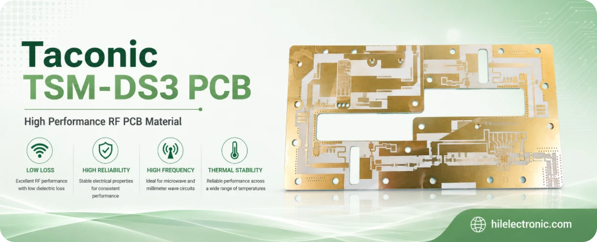
Компанія Highleap Electronics виготовляє та збирає друковані плати Taconic TSM-DS3 для радарів, фазованих решіток, аерокосмічних радіочастотних пристроїв (ATE), підсилювачів, фільтрів, аерокосмічних радіочастотних пристроїв та великоформатних багатошарових матеріалів. Кошторис зосереджений на повній конструкції — осердях TSM-DS3, сполучному матеріалі, товщині пресування, реєстрації, свердлінні, гальванічних покриттях, пробних відбитках, складанні та екологічній прийнятності, — а не лише на технічному описі ламінату.
Багатошаровий осцилоскоп TSM-DS3 у Highleap
Highleap підтримує багатошарові радіочастотні конструкції з низькими втратами, побудовані за допомогою TSM-DS3, включаючи PTFE або гібридні конструкції, контрольований імпеданс, послідовне ламінування, щільні структури переходних отворів та вдосконалені структури з'єднань між шарами, коли розглядається повне стекування. Великі панелі, незвичайні лінії з'єднань, тонкі діелектричні відстані та критична для радіочастот реєстрація оцінюються на основі фактичної конструкції, а не загальної діаграми можливостей.
Важливо: Збірки TSM-DS3 можуть бути підтримані як інженерними зразками, так і кваліфікаційними партіями, а також багатосерійним виробництвом. Проекти з високими вимогами до теплових, фазових, надійних або взаємоз'єднань проходять перевірку процесу перед затвердженням остаточного маршруту збірки.
Найкраще підходить
Температурно-чутливі радари та фазовані решітчасті решітки, інтерфейсні плати ATE, високошарові радіочастотні прилади, фільтри, підсилювачі та аерокосмічна електроніка.
Головна помилка
Розгляд стабільного ламінату як гарантії стабільної роботи продукту без визначення міді, з'єднання, температурних градієнтів, корпусу, складання та випробувань.
Обсяг виробництва
Перевірка матеріалів, проектування стекування та ліній з'єднань, обробка PTFE, масштабування, контрольований імпеданс, перехідні отвори, складання та кваліфікація, визначена замовником.
Вхідні дані для цитат
Деталі осердя/препрега, товщина пресування, обмеження по радіочастотному та температурному впливу, структура, розміри, кількість, комплектація та план випробувань.
Коли TSM-DS3 є кращим радіочастотним матеріалом
Taconic TSM-DS3 — це ламінат з PTFE з низькими втратами, наповнений керамікою та невеликою кількістю скловолокна, армованого скловолокном. AGC оголошує номінальний коефіцієнт теплопровідності Dk 3.0 ± 0.05, теплопровідність приблизно 0.65 Вт/м·K та підкреслює діелектричну стабільність за температури. Його комерційна цінність полягає не просто в «низьких втратах». Це поєднання передбачуваності радіочастотних перепадів, теплових властивостей, армування та багатошарової придатності.
Оберіть TSM-DS3, коли
- фаза, імпеданс або резонанс повинні залишатися передбачуваними за будь-якої температури;
- друкована плата велика, має багато шарів або вимоглива до механічних вимог;
- характеристики радара, фазованої решітчастої решітки, підсилювача, фільтра або АТЕ залежать від повторюваної діелектричної відстані;
- можна кваліфікувати сумісну систему з'єднання з низькими втратами.
Виберіть інший матеріал, коли
- основною метою є найнижчий можливий Dk для ефективності антени;
- звичайний FR-4 або термореактивний сталь з низькими втратами вже відповідає екологічним вимогам та бюджету каналу;
- конструкція не має визначених вимог до температури чи фази;
- замовник не може затвердити повну конструкцію серцевини/препрега.
TSM-DS3 часто стає цінним після того, як розробник виявляє системну проблему — температурно-залежну фазу, нестабільний резонанс, реєстрацію на великій панелі або складний багатошаровий радіочастотний сигнал — не лише тому, що продукт працює на високій частоті.
Виробничі можливості для багатошарових матеріалів TSM-DS3
Highleap може перевірити жорсткі радіочастотні плати, багатошарові конструкції TSM-DS3 та гібридні стеки. Проекти можуть включати fastRise 27 або інший схвалений скріплювальний матеріал, послідовне ламінування, нанесення наскрізних отворів, глухі або лазерно-свердлені конструкції, контрольований імпеданс та складання "під ключ". Кожен елемент підтверджується фактичним проектом; жодна сторінка зі загальними матеріалами не може встановити можливу кількість шарів або структуру переходів.
| Виробнича зона | Огляд інженерії Highleap | Потрібне рішення клієнта |
|---|---|---|
| Серцевина та лінія з'єднання | Перевірте товщину сердечника TSM-DS3, мідь, сполучний матеріал, кількість шарів, товщину пресування, потребу в смолі та симетрію. | Затвердити остаточний варіант стека та будь-які зміни в конструкції, що підлягають придбанню. |
| Масштабування та реєстрація панелі | Плануйте рух матеріалу, баланс міді, цілі для інструментів, послідовність ламінування та суміщення шарів. | Визначте критичне радіочастотне вирівнювання, порожнини, масиви, роз'єми та механічні опорні точки. |
| Свердління та нанесення покриття | Визначте активацію PTFE, маршрут свердління, мідь до стінки отвору, співвідношення сторін, стадії заповнення перехідних отворів або мікроперехідних отворів, а також відбір проб поперечного перерізу. | Забезпечити через клас надійності та будь-які вимоги щодо термічного циклу або IST. |
| Радіочастотний контроль | Змодельуйте імпеданс на основі фактичної конструкції та плану фази, резонатора, внесених втрат або спеціальних замовлень замовника. | Вкажіть параметр приймання, частоту, допуск та метод випробування. |
| збірка | Перегляньте масові роз'єми, екрануючі корпуси, термоінтерфейси, оплавлення, підтримку плат, очищення та доступ для тестування. | Надайте специфікацію матеріалу, механічне креслення, випробувальне пристосування та екологічні вимоги. |
Можливе замовлення прототипів, малосерійного та повторного виробництва. Перехід до виробництва вимагає ідентифікації замороженого матеріалу, конструкції преса, даних масштабування та критеріїв випуску; інакше кожна партія стає новим експериментом.
Вимоги до проектування для забезпечення стабільної за температури радіочастотної продуктивності
Фраза «температурно-стабільний ламінат» не визначає характеристики виробу. На реакцію плати також впливають розширення міді, напруження в корпусі, паяні з'єднання, роз'єми, компоненти, потік повітря та розподіл тепла. Тому в запиті цінових пропозицій (RFQ) вимоги до навколишнього середовища мають бути перетворені на вимірювані критерії плати або виробу.
Забезпечте ці електричні та теплові входи
- діапазон робочих температур та температур зберігання;
- допустима зміна імпедансу, фази, затримки, резонансу або внесених втрат залежно від температури;
- діапазон частот, рівень потужності, робочий цикл та локальні джерела тепла;
- опорна площина, роз'єм, антена та калібрувальні структури;
- теплові інтерфейси, металеві носії, теплорозподільники, монтажний момент та обмеження корпусу;
- необхідні випробування на циклічну зміну температури, ударні навантаження, випалювання або функціональні випробування;
- кореляція купона з продуктом та метод деембеддингу клієнта.
Highleap може виготовляти вироби відповідно до цих вимог, але кваліфікація на рівні системи з радіочастотними та тепловими характеристиками залишається спільним інженерним завданням. Результат вимірювання імпедансу голої плати за кімнатної температури сам по собі не може довести продуктивність фазованої решітки в усьому робочому діапазоні.
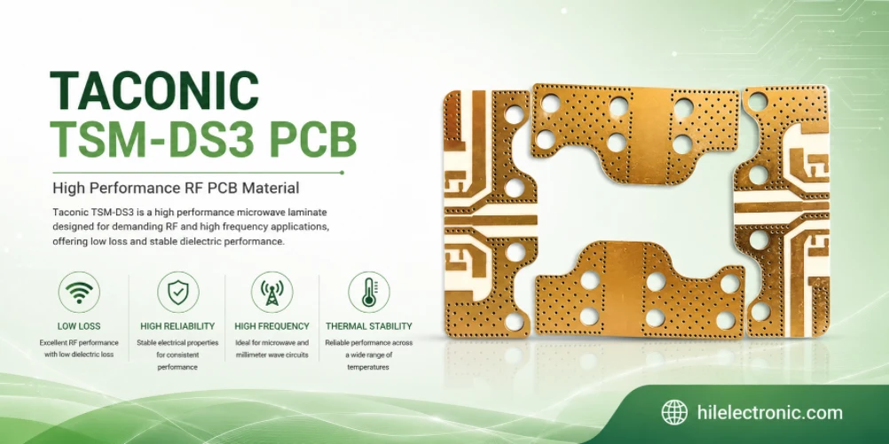
Збірка TSM-DS3 з використанням fastRise 27 або інших склеювальних матеріалів
У багатошаровій радіочастотній друкованій платі лінія затвердіння є електричним шаром. Її товщина створюється під час ламінування та залежить від конструкції препрега, відсотка міді, топографії, тиску, температури, вакууму, розміру панелі та течії смоли. Товщина необробленого шару не є гарантованим кінцевим діелектричним відстанню.
- Підтвердіть сумісність. Перевірте вибраний сполучний матеріал за допомогою поверхонь TSM-DS3, обробки міді, циклу затвердіння, історії температур та суміжних матеріалів.
- Карта попиту на смолу. Перевірте щільність міді, великі прозорі області, порожнини, області заповнення переходних отворів та висоту локальних елементів.
- Встановіть цільові показники товщини пресування. Використовуйте доступні конструкції шарів та виробничі дані, а не ідеалізоване номінальне значення.
- Плануйте послідовне ламінування. Враховуйте кожен цикл пресування та сукупний термічний вплив на осердя, гальванічні елементи та мікровідверстия.
- Контролюйте просторовий рух. Застосовуйте цільові показники масштабування та реєстрації на основі повного пакету друкарських машин.
- Співвіднесіть купони. Переконайтеся, що на купоні зображено ті ж матеріали, мідь, цикл пресування та покриття, що й на функціональній схемі.
Для отримання додаткової інформації див. посібник з проектування препрегів та радіочастотних переходних отворів fastRise 27 від Highleap.
Застосування: Що вирішує матеріал у продукті
Фазова решітчаста та радіолокаційна електроніка
Продуктивність масиву залежить від фазової узгодженості, повторюваної геометрії подачі, температурної поведінки та реєстрації на великій панелі. TSM-DS3 може задовольнити ці вимоги, коли замовник також контролює геометрію елементів, роз'єми, радом, калібрування та температурні градієнти на рівні продукту.
Структури інтерфейсу ATE та карт зондів
Великий розмір плати, велика кількість шарів, щільні переходні отвори, контрольований імпеданс, механічна площинність та термоциклування можуть зустрічатися разом. У проекті слід вказувати, які розміри та електричні шляхи контролюють точність кріплення; застосування жорстких допусків всюди без потреби збільшує вартість.
Підсилювачі, фільтри та аерокосмічна радіочастотна система
Низькі втрати та температурна стабільність можуть зменшити дрейф, але щільність потужності, заземлення, надійність гальванічного отвору, механічне кріплення та чистота складання залишаються критично важливими. Ламінат є однією з частин плану контролю.
Багатошарові радіочастотні матеріали великого формату
Армування та поведінка матеріалу можуть підтримувати конструкції з вимогливими розмірами, але баланс міді, послідовність пресування, масштабування панелі, свердління та підтримка складання повинні бути розроблені спеціально для розміру плати.
Фактори вартості та часу виконання
| Фактор | Чому це важливо? | Комерційний контроль |
|---|---|---|
| Конструкція з сердечника/препрегу | Незвичайна товщина, багатошаровість або спеціальні сполучні плівки впливають на закупівлю та кваліфікацію преса. | Затверджуйте доступні конструкції заздалегідь. |
| Кількість шарів та цикли пресування | Більша кількість циклів підвищує сумісність, заповнення смолою, надійність переходних отворів та ризик зміни розмірів. | Використовуйте мінімальну архітектуру, яка відповідає вимогам маршрутизації та ізоляції. |
| Розмір плати та вирівнювання радіочастотних сигналів | Великі панелі потребують масштабування, підтримки, контролю площинності та додаткового контролю. | Визначте критичні опорні точки та реалістичні допуски. |
| Сліпі переходні отвори та мікроперехідні отвори | Лазерне свердління, заповнення, послідовне ламінування та купони на надійність додають етапи процесу. | Використовуйте HDI лише там, де цього вимагає прорив або радіочастотний перехід. |
| Кваліфікація щодо температури/радіочастотних характеристик | Екологічні камери, пристосування, калібрування, аналіз даних та повторні зразки збільшують витрати та збільшують терміни. | Визначте точний план приймальних випробувань та вибірки. |
| Складність складання | Великі BGA, прес-роз'єми, екрани, носії та термоінтерфейси можуть домінувати в загальній вартості друкованих плат. | Надішліть дані щодо складання та механіки разом із запитом цінових пропозицій на голу плату. |
Для точного виготовлення необхідно перевірити терміни виконання матеріалів та мінімальні обсяги замовлення. Highleap не надаватиме цінову пропозицію на перший погляд швидкий прототип, використовуючи один стек, і непомітно переноситиме виробництво на інший.
Що потрібно подати для отримання комерційної пропозиції TSM-DS3
Надайте точний клас TSM-DS3 та товщину осердя, тип та вагу міді, матеріал з'єднання, повний стек, цільові значення товщини пресування, таблицю імпедансу, діапазон частот, межі фаз або втрат, робочу температуру, архітектуру переходних отворів, критичні розміри реєстрації, розмір плати та панелі, обробку поверхні, кількість, прогноз, цільові показники доставки та вимоги до якості/випробувань.
Для складання додайте специфікацію матеріалу (BOM), центроїд, креслення, деталі роз'єму та екрану, термоінтерфейси, межі паяння та очищення, покриття, доступ для випробувань, інформацію про кріплення, профіль навколишнього середовища та очікувані показники звітності.
Корисним результатом роботи Highleap є пакет рішень щодо виробництва: наявність матеріалів, запропоноване складання штабелів, питання технологічності, необхідні схвалення замовника, маршрут процесу, дані перевірки/випробування, фактори витрат та ризики, пов'язані з термінами виконання. Саме це потрібно покупцеві, щоб вирішити, чи може завод виготовити продукт.
Комерційні поширені запитання
Чи може Highleap виготовити багатошарову друковану плату Taconic TSM-DS3?
Так, можна розглянути відповідні багатошарові та гібридні проекти TSM-DS3. Остаточна доцільність залежить від сполучного матеріалу, товщини пресування, кількості шарів, розмірів, архітектури переходних отворів, реєстрації, складання та вимог до випробувань.
Чи TSM-DS3 кращий за TLY-5?
Зазвичай ні. TSM-DS3 часто вибирають за температурну стабільність та багатошарову передбачуваність; TLY-5 є привабливим для антен з дуже низьким Dk та низькими втратами або структур міліметрового діапазону. Вибирайте за вимогами до продукту, а не за простим ранжуванням.
Чи можна використовувати fastRise 27 як сполучний матеріал?
Це може бути придатним для перевірених конструкцій, але для повного комплексу необхідно перевірити сумісність, кількість шарів, потребу в смолі, товщину пресування, цикл пресування та кумулятивну історію нагрівання.
Які тести можна включити?
Залежно від проекту, кошторис може включати електричні випробування, перевірку критичних розмірів, мікрошліфування, імпедансний контроль, резонаторні або фазові випробування, термоциклування, AOI/рентгенівське дослідження, функціональні випробування або радіочастотні випробування, визначені замовником.
Як визначається ціна?
Ціна залежить від матеріалу конструкції, розміру плати, кількості шарів, циклів пресування, структури переходних отворів, критичних допусків, кількості, складності складання та необхідних радіочастотних або екологічних доказів. Надішліть повний пакет даних для отримання твердої цінової пропозиції.

Рекомендовані повідомлення

Друкована плата Taconic RF 35 проти RO4350B
ЗмістRF-35 проти RO4350B Закупівлі та...

Виробництво друкованих плат фільтра TMM4
Виробництво друкованих плат фільтра TMM4 контролюється...

Виготовлення друкованих плат TMM6
Виготовлення TMM6 – це сторінка контролю процесу для середньої Dk...

Виробництво друкованих плат TMM3 для радіочастотних модулів
Виробництво друкованих плат TMM3 найбільш корисне там, де радіочастотний модуль...
Як отримати цінову пропозицію на друковані плати
Давайте проведемо для вас аналіз DFM/DFA та надамо вам звіт. Ви можете безпечно завантажити свої файли через наш вебсайт. Нам потрібна наступна інформація, щоб надати вам цінову пропозицію:
-
- Gerber, ODB++ або .pcb, спец.
- Список специфікації, якщо вам потрібна збірка
- Кількість
- Час повороту
Для послуг з виготовлення друкованих плат (PCBA), будь ласка, надайте свою специфікацію матеріалів (BOM) та будь-які конкретні інструкції зі складання. Ми також пропонуємо аналіз DFM/DFA для оптимізації ваших конструкцій для технологічності та складання, забезпечуючи безперебійний виробничий процес.