
Ábhar PCB EM-892K: Treoir Déantúsaíochta do PCBanna Ardluais, AI, HPC agus 5G
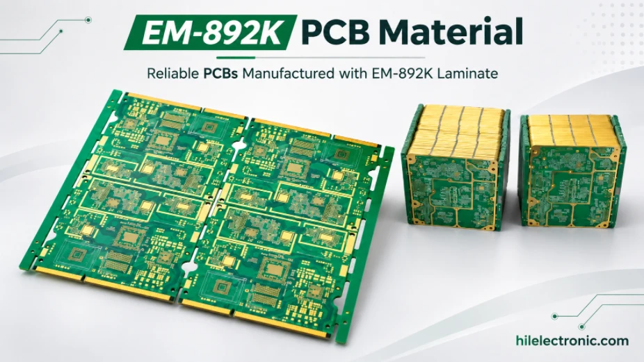

Looking for a PCB manufacturer to build boards using Ábhar PCB EM-892K? Highleap Electronics manufactures custom PCBs and provides PCB assembly for customer-defined material and design requirements. We do not manufacture EM-892K laminate. We review the specified construction, stackup, electrical requirements and production files, then assess the feasibility of manufacturing the finished PCB or PCBA.
EM-892K is positioned by Elite Material for high-speed Ethernet, networking, HPC, AI, 5G and antenna applications. For a production quotation, the important details are the exact material construction, layer stackup, impedance requirements, drilling and via design, board quantity, and whether assembly is also required.
EM-892K PCB Manufacturing at Highleap
Highleap supports customers who need a finished multilayer PCB manufactured to an EM-892K material requirement. Our scope is PCB fabrication and, when required, downstream SMT/THT assembly—not the production of the laminate itself.
Before accepting a build, the manufacturing team needs to confirm:
- Exact material: EM-892K or EM-892BK, including the specified laminate/prepreg construction and any approved material alternatives.
- Soláthar ábhar: Whether the customer will provide the material or whether sourcing is required and can be confirmed.
- Tógáil an bhoird: Layer count, finished thickness, copper weights, dielectric build and via structure.
- Ceanglais leictreacha: Controlled-impedance layers, target values, tolerances and any required verification.
- Raon feidhme an ordaithe: Bare PCB only or a complete PCBA with component sourcing, assembly and testing.
This information allows Highleap to assess the actual manufacturing requirement instead of quoting from the material name alone. For related low-loss material projects, see our roghnú ábhar PCB ardluais treoir.
EM-892K Material Data to Confirm Before Production
The Elite Material EM-892K/EM-892BK datasheet (Rev. July 2024) identifies the material as high-Tg, extreme-low-loss and halogen-free. The following are published typical values, not guaranteed values for every laminate construction or finished PCB.
| Maoin | Published typical value | Test condition / method |
|---|---|---|
| Tg | 180°C (TMA); 215°C (DMA) | Different test methods; values are not interchangeable |
| Dk ag 1 GHz | 3.11 / 2.93 | R/C 55/70%; IPC-TM-650 2.5.5.9 |
| Dk ag 10 GHz | 3.00 / 2.84 | R/C 55/70%; cavity resonator / SPC |
| Df ag 1 GHz | 0.0014 / 0.0012 | R/C 55/70%; IPC-TM-650 2.5.5.9 |
| Df ag 10 GHz | 0.0019 / 0.0017 | R/C 55/70%; cavity resonator |
| Td | 420 ° C | TGA, 5% weight loss |
| T288 | >60 min (clad and etched) | IPC-TM-650 2.4.24.1 |
The paired Dk/Df values correspond to the datasheet’s 55% / 70% resin-content conditions. At 10 GHz, the datasheet also lists Df values of 0.0015 / 0.0013 using the SPC method. Use the value and test method agreed by the design team; do not mix results from different methods in one design calculation.
For fabrication, the key point is to confirm the exact construction and the customer’s approved material specification. Dk and Df are reference inputs for electrical design; they do not define the finished trace impedance on their own. Review the Elite Material EM-892K/EM-892BK datasheet alongside the released stackup and fabrication notes.
EM-892K Stackup and Controlled-Impedance Review
For a controlled-impedance EM-892K board, the PCB manufacturer needs the complete stackup—not just a note saying “use EM-892K.” The stackup should define the layer sequence, laminate/prepreg construction, dielectric thicknesses, copper weights, reference planes and finished board thickness.
Before production, Highleap should review the following against the customer’s design data:
- Single-ended and differential impedance targets, including tolerance.
- Signal-layer assignments and the corresponding reference planes.
- Dielectric thickness and the exact resin/glass construction used in the stackup.
- Finished copper thickness, trace width and spacing assumptions.
- Via types, drill sizes, aspect ratios and any backdrilling requirements.
- Impedance coupons and the requested verification method, where specified.
These details affect both electrical performance and manufacturing feasibility. Highleap’s Innealtóireacht cruachta sraithe PCB review can be used to evaluate the proposed construction. If the design requires removal of unused via stubs, specify the relevant layers and depth requirements for Druileáil siar PCB; it should be treated as a design-specific requirement, not an automatic process step.
EM-892K Multilayer PCB Fabrication and Quality Control
Once the construction is approved, the board must be manufactured to the released stackup and fabrication drawing. For an EM-892K multilayer build, the quotation and DFM review should make the critical process requirements visible before production starts.
- Lamination and registration: Confirm the core/prepreg layup, finished dielectric thickness, press construction and layer-registration requirements.
- Drilling and via formation: Review hole sizes, aspect ratios, via structures and any controlled-depth drilling specified in the design.
- Hole preparation and plating: Define the required desmear and copper-plating quality for reliable interlayer connections.
- Pattern and dimensional control: Check copper geometry, board dimensions, finished thickness and registration tolerances against the fabrication data.
- Inspection and electrical verification: Identify the required inspection, electrical test, impedance verification and acceptance criteria in the RFQ.
Elite Material describes EM-892K as having multiple-lamination capability and resin suitable for hybrid constructions with mid-loss materials. If a hybrid stackup is proposed, the complete combination must be engineered and approved; do not substitute materials or resin systems without customer authorization. Highleap’s monarú PCB ilchiseal service is the relevant manufacturing scope for this review.
EM-892K PCB Assembly and Turnkey PCBA
If the requirement is a finished electronic assembly rather than bare boards, define the PCBA scope at the quotation stage. Highleap provides Tionól PCB services, including SMT/THT production, inspection and testing according to the project requirements.
The laminate grade does not by itself determine solder-joint quality or assembly yield. For the assembled product, the PCB revision, pad geometry, surface finish, board flatness, component package mix and assembly process must all be considered together.
For a combined PCB and PCBA quotation, provide the BOM, pick-and-place file, assembly drawings, polarity/orientation details and any special inspection or functional-test requirements. Highleap’s tionól PCB turnkey service can be considered when the project requires PCB fabrication, component sourcing and assembly through one manufacturing workflow.
Request an EM-892K PCB Manufacturing Quote
To receive a useful quotation, send the files and requirements that define the actual build. A material name alone is not enough to determine the manufacturing route, material sourcing, stackup or final cost.
- Sonraí PCB: Gerber or ODB++ files, NC drill files and fabrication drawing.
- Sonraíocht ábhair: EM-892K or EM-892BK designation, approved laminate/prepreg construction and datasheet revision.
- Cruachta: Layer count, finished thickness, copper weights, dielectric thicknesses and reference-plane arrangement.
- Ceanglais leictreacha: Impedance values and tolerances, controlled layers, test coupons and backdrilling details if required.
- Sonraí an ordaithe: Quantity, prototype or production stage, delivery target and inspection/acceptance requirements.
- PCBA files, if needed: BOM, pick-and-place data, assembly drawings and test requirements.
- Soláthar ábhar: Confirm whether the material is customer-supplied or needs to be sourced for the order.
PCB Fabrication · PCB Assembly
Need a Factory for Your EM-892K PCB Project?
Send your stackup, fabrication files, material specification and quantity. Highleap can review the manufacturing package and confirm the feasible PCB or PCBA scope, including material-sourcing requirements.

Poist is molta
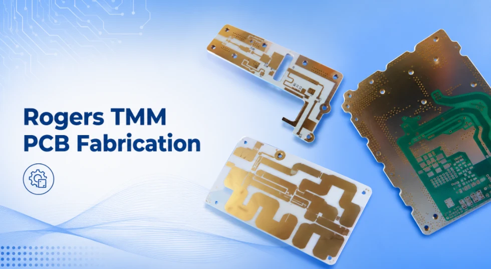
Déantúsaíocht PCB TMM
Clár Ábhair Raon Feidhmiúcháin PCB TMM le haghaidh RF agus...

RT duroid 6002 PCB Athfhriotail agus Stackup
Is leis an leathanach seo an tasc luachana agus sainmhínithe cruachta...
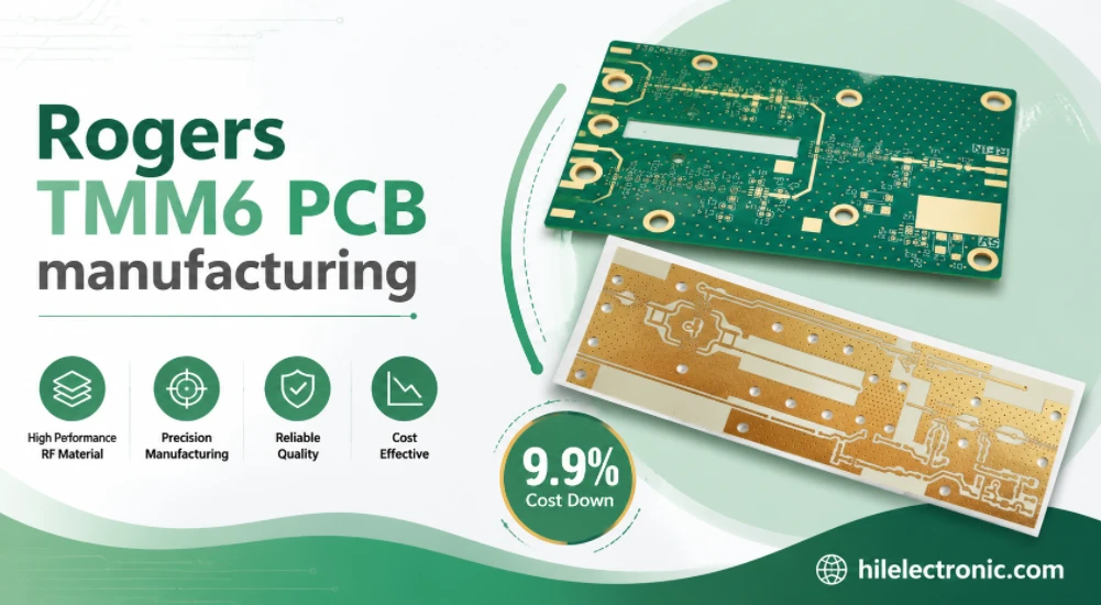
Déantúsaíocht PCB Scagaire TMM6
Clár ÁbhairCén Fáth a nÚsáideann Dearthóirí Scagairí Micreathonnta...
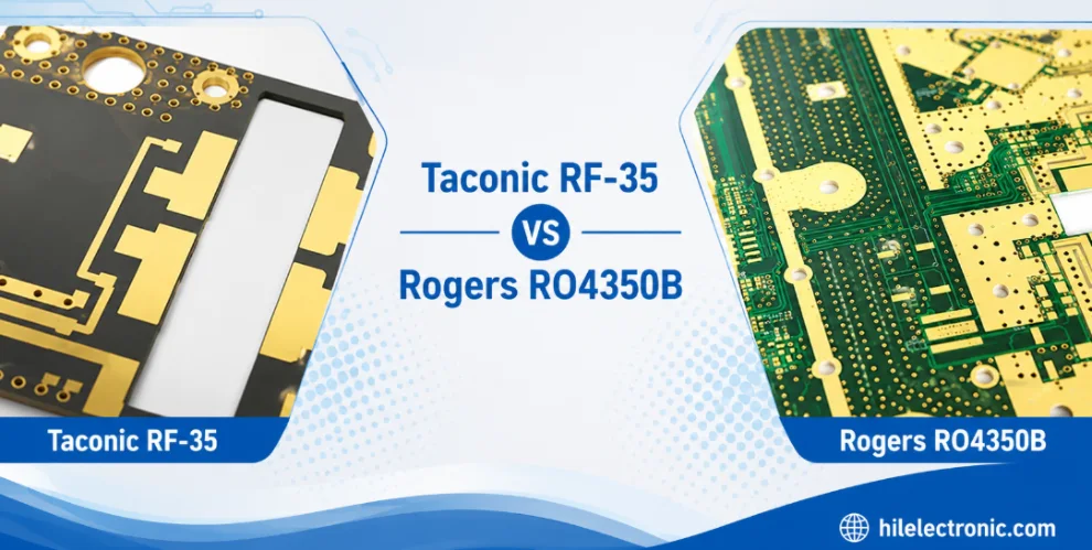
Taconic RF 35 i gcomparáid le PCB RO4350B
Clár ábhair Soláthar agus...RF-35 vs RO4350B
Conas luachan a fháil le haghaidh PCBanna
Déanaimis anailís DFM/DFA a dhéanamh duit agus rachaimid ar ais chugat le tuarascáil. Is féidir leat do chuid comhad a uaslódáil go slán tríd ár suíomh Gréasáin. Teastaíonn an fhaisnéis seo a leanas uainn chun luachan a thabhairt duit:
-
- Gerber, ODB++, nó .pcb, sonraíocht.
- Liosta BOM má tá cóimeáil uait
- Cé mhéad
- Cas am
I gcás seirbhísí PCBA, cuir do Bhille Ábhar (BOM) agus aon treoracha tionóil sonracha ar fáil. Cuirimid anailís DFM/DFA ar fáil freisin chun do dhearaí a bharrfheabhsú le haghaidh inmhonaraitheachta agus tionóil, rud a chinntíonn próiseas táirgthe réidh.