
IT-258GA3 PCB Material Properties and Applications
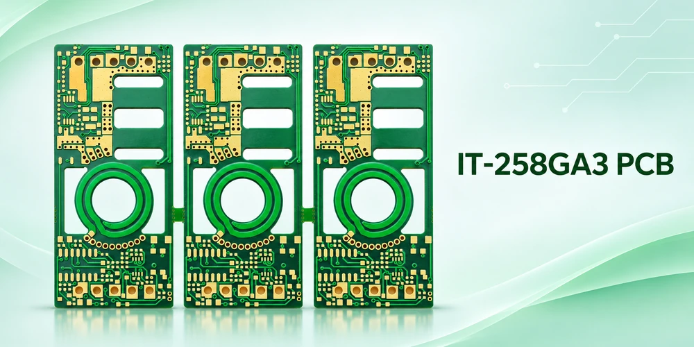
Illustration of heavy-copper PCB panel layouts.
ITEQ IT-258GA3 is a halogen-free, medium-Tg laminate and prepreg system for rigid multilayer boards, including automotive ECUs and heavy-copper builds. Its datasheet lists 155°C Tg by DSC, a CTI of 400–599 V (class 1) and thermal conductivity of 0.70 W/m·K. These properties support three separate design checks: how the copper carries current, how the board maintains insulation and how the assembly removes heat.
Treat creepage, clearance and internal CAF as different paths
Comparative tracking index (CTI) describes how an insulating material behaves in a standardized contaminated-surface tracking test. CTI class 1 in the ITEQ sheet does not specify a safe board operating voltage. Determine creepage along exposed insulating surfaces from the governing product requirements and the applicable material group, working voltage and pollution degree. Determine clearance through air from the applicable voltage stresses, overvoltage and altitude considerations. Confirm any assumptions about coating, slots and barriers against the governing standard rather than assigning a universal spacing from the laminate name.
Conductive anodic filament (CAF) growth is a separate failure mechanism. Moisture can enter paths along the resin-to-glass interface; with electric bias and susceptible geometry, conductive growth can develop internally between conductors. Closely spaced plated holes or holes next to internal copper are important review points. Layout spacing, drill-induced damage, the construction and the moisture/bias environment all matter. Consult IEC 60664 1- for insulation coordination where it applies. It does not replace a product-specific qualification plan for buried conductor spacings.
ITEQ describes CAF resistance with a 1000 V claim in the sheet’s feature summary but does not publish the test spacing, humidity and duration there. For a product qualification, define the coupon’s conductor geometry, test bias and moisture exposure, observation period and insulation-resistance acceptance. A dry finished-board opens-and-shorts test does not answer that question. Conversely, a good humidity-bias result on a bare-board coupon does not qualify surface contamination or assembly residues on the populated product. When selecting a Ábhar PCB atá frithsheasmhach in aghaidh CAF, decide which failure geometry the coupon must represent.
Specify the copper that remains after etch and plating
“4 oz copper” does not say whether the callout is starting foil or finished copper, which layers it covers, or how the narrowest current-carrying section is accepted. A power net may cross a wide plane, narrow through a connector or fuse footprint, then change layers through a plated-via array. The highest current density can occur at the neck or at the vias even when the plane itself has low resistance.
Hypothetical resistance check. A straight copper neck 20 mm long, 2.0 mm wide and 70 µm thick has an ideal room-temperature resistance of about 2.5 mΩ using 1.72 × 10⁻⁸ Ω·m for copper. At 10 A DC it dissipates about 0.25 W. If the effective width falls to 1.5 mm at the same thickness, the estimate rises to about 3.3 mΩ and 0.33 W. The simple rectangular model ignores taper, plated variations, vias and solder joints. It predicts resistive heating, not allowable current or temperature rise.
For production, state the finished copper requirement per layer, the critical conductor widths and spacings after etch, and the via-wall acceptance. On external layers, distinguish base foil from any plating contribution. In thick copper, lateral etching can narrow a trace and change sidewall shape; pattern plating can produce different thicknesses in sparse and dense areas. Review the finished section at a representative constriction and the plated transition, not only on a large test pad. IPC-2152 supplies a framework for current-carrying capacity. Apply an appropriate model or measurement for the actual copper paths, adjacent planes, ambient conditions and allowed rise.
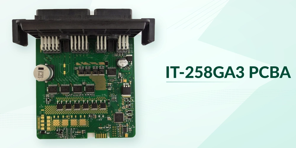
PCBA illustration with a connector and populated board. Current paths and solder requirements depend on the design.
Review the lamination and thermal path together
Heavy inner copper creates cavities where adjacent copper was etched away. A thicker foil does not automatically mean a thicker finished dielectric above the trace; prepreg resin has to fill the cavities and keep adequate separation over the copper. Compare resin demand at dense copper, large cleared areas and isolation boundaries. Check the actual pressed spacing and resin fill on representative sections, especially at abrupt copper-density changes. A balanced heavy-copper stack-up should also be reviewed for panel flatness and the plating challenge at thick-board through holes.
Draw the heat path from each power device through its package attachment, copper spreading area, any thermal vias and the interface to the enclosure or heatsink. The laminate conductivity is just one part of that network. A thin dielectric over a useful spreading plane and a thick dielectric behind a small device can yield very different temperatures even with the same resin system. At first article, measure under representative current, enclosure and airflow conditions. Watch for connector necks and layer transitions as well as the power device itself.
DÉANTÚ & TIONÓL PCB
Planning an IT-258GA3 PCB build?
Highleap can review the board construction and assembly requirements together.
Include finished copper requirements, insulation constraints and connector soldering details.
IT-258GA3TC is the laminate designation
In the current ITEQ sheet, IT-258GA3TC identifies the copper-clad laminate for the IT-258GA3 system; IT-258GA3BS identifies its prepreg. Use those designations to check the stack-up and purchasing description. The grade is a candidate for thick copper and insulation-sensitive rigid boards; the 10 GHz datasheet values also help screen whether a long high-speed route needs a separate material decision.
| Maoin | ITEQ value | Basis or limitation |
|---|---|---|
| Tg and MOT | 155°C Tg; 130°C MOT | DSC and UL 746, respectively |
| Comparative tracking index | Class 1 (400–599 V) | ASTM D3638 / UL 746 as listed; test classification |
| Seoltacht theirmeach | 0.70 W / m · K. | ITEQ feature summary; not a populated-board thermal resistance |
| Leathnú ais-Z | 2.8% from 50°C to 260°C | IPC-TM-650 2.4.24; laminate specimen |
| Dk / Df at 10 GHz | 4.3 / 0.016 | 50% resin content; IPC-TM-650 2.5.5.13 |
Bring the connector and solder process into the release
Large copper planes can draw heat out of a soldered terminal while nearby SMT parts heat much faster. In heavy-copper PCB assembly, review thermal reliefs, solder fill and heat exposure with the mechanical and electrical constraints in view. An isolated thermal relief may make the joint easier to solder but can constrict the current path. If a connector instead uses press-fit pins or a bolted connection, coordinate the hole tolerances and insertion or clamping loads with the board stack and support.
Le haghaidh Highleap PCB and assembly quotation, identify the finished copper by layer, send the current waveform and allowable rise, and show the working-voltage and transient requirements with the insulation boundaries. Include plated-hole requirements, terminal drawings, the BOM and the needed evidence for first article. This lets Highleap Electronics review the copper geometry, press construction and assembly process against the same product requirements.

Written by:
Ashley
Bainisteoir Sinsearach Gnó Idirnáisiúnta ag Highleap Electronics
Speisialtóireacht Ashley is ea réitigh aon-stad PCB agus PCBA, ag tacú le custaiméirí idirnáisiúnta le hanailís DFM, optamú comhad Gerber, agus comhordú innealtóireachta ó mhonarú PCB go táirgeadh EMS.
Le scileanna cumarsáide teicniúla láidre agus Béarla líofa aici, oibríonn sí go dlúth le foirne innealtóireachta chun intinn dearaidh, próisis déantúsaíochta agus ceanglais cháilíochta a ailíniú—ag cuidiú le seachadadh iontaofa a chinntiú do thionscadail chasta PCB agus PCBA.

Poist is molta
PCB IT-968GSE le haghaidh Líonrú Ardluais
Léaráid PCB IT-968GSE le haghaidh lasc thar a bheith ísealchaillteanais agus...
Boird IT-602G HDI a Thógáil le haghaidh SSDanna agus Modúil Chuimhne
Samplaí PCB IT-602G le haghaidh HDI, SSD agus modúl cuimhne...
PCBanna Cúlphlána IT-988GL le Rialú Próisis Íseal-CTE
Déantúsaíocht PCB ilchiseal IT-988GL...
PCB Arlon 85NT: Déantúsaíocht Polaimíde agus Rialú SMT
Léaráid déantúsaíochta PCB; grád ábhair agus...
Conas luachan a fháil le haghaidh PCBanna
Déanaimis anailís DFM/DFA a dhéanamh duit agus rachaimid ar ais chugat le tuarascáil. Is féidir leat do chuid comhad a uaslódáil go slán tríd ár suíomh Gréasáin. Teastaíonn an fhaisnéis seo a leanas uainn chun luachan a thabhairt duit:
-
- Gerber, ODB++, nó .pcb, sonraíocht.
- Liosta BOM má tá cóimeáil uait
- Cé mhéad
- Cas am
Chomh maith le monarú PCB, cuirimid réimse cuimsitheach seirbhísí leictreonacha ar fáil, lena n-áirítear dearadh PCB, PCBA, agus réitigh lán-eochair. Cibé an bhfuil cabhair uait le fréamhshamáirí, fíorú dearaidh, foinsiú comhpháirteanna, nó olltáirgeadh, soláthraímid tacaíocht ó cheann ceann go ceann chun rath do thionscadail a chinntiú.
I gcás seirbhísí PCBA, cuir do Bhille Ábhar (BOM) agus aon treoracha tionóil sonracha ar fáil. Cuirimid anailís DFM/DFA ar fáil freisin chun do dhearaí a bharrfheabhsú le haghaidh inmhonaraitheachta agus tionóil, rud a chinntíonn próiseas táirgthe réidh.