
ඝන බහු ස්ථර විශ්වසනීයත්වය සඳහා Shengyi S1000-2M PCB
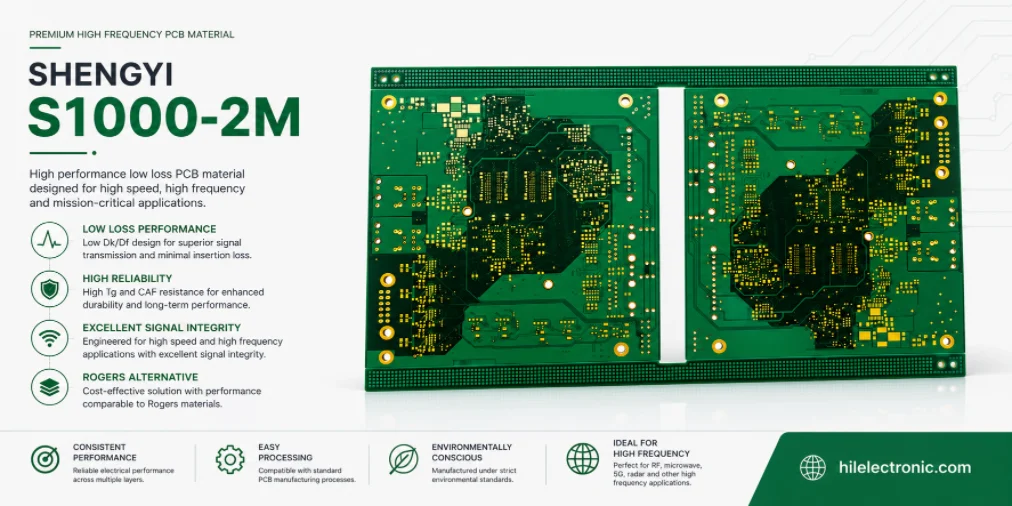
Shengyi S1000-2M is a high-Tg, low-CTE FR-4.0 laminate for ඉහළ ස්ථර ගණන් පුවරු that must survive lead-free processing and maintain plated-through-hole and insulation reliability. Shengyi highlights 180°C Tg by DSC, 185°C by DMA, 355°C Td, 41 ppm/°C z-axis CTE below Tg, 208 ppm/°C above Tg, 2.4% total z expansion from 50–260°C, T260 greater than 60 minutes, T288 of 30 minutes, anti-CAF performance, low water absorption, and suitability for computer, communication, automotive, and high-multilayer products.
The material should not be positioned as an ultra-low-loss laminate. Shengyi’s public data list typical Dk 4.6 and loss tangent 0.018 at 1 GHz on the stated reference specimen. The primary value is thermal-mechanical reliability in thick multilayers. A reliable S1000-2M board still needs conservative hole geometry, controlled drilling and desmear, uniform plating, copper balance, registration, moisture management, and a defined assembly history.
Why High Layer Count Magnifies Every Thermal-Mechanical Risk
Each additional layer adds interfaces, copper distribution, registration opportunities, dielectric thickness tolerances, and lamination history. High-layer boards are also often physically larger and thicker, with more connectors and through holes. That means the same material property variation creates a larger absolute effect.
| High-layer effect | Risk created | පාලන උපාය මාර්ගය |
|---|---|---|
| Greater finished thickness | Longer PTH barrels and larger total z expansion. | Use conservative hole sizes/aspect ratios, low-CTE material, robust plating, thermal qualification. |
| More inner-layer interfaces | More opportunities for resin starvation, voids, treatment failure, or registration error. | Resin-demand analysis, copper balance, press recipe, panel-position cross-sections. |
| More copper imbalance | Warpage, local thickness variation, uneven pressure and heating. | Symmetric stack, copper balancing/thieving, controlled panel design. |
| More via fields/connectors | Dense holes increase CAF paths and plating demand. | Spacing/voltage rules, drill/desmear control, plating distribution, anti-CAF qualification. |
| More routing layers | More layer changes and backdrill structures. | Via topology planning, residual-stub control, registration and inspection. |
| More thermal mass | Longer or uneven assembly heating and cooling. | Board-temperature profiling at heavy copper and connector regions. |
S1000-2M reduces several material-side risks, particularly expansion and thermal endurance. It does not simplify the geometry. A high-layer release should begin with the board’s worst structures: smallest finished hole, thickest local copper, deepest backdrill, densest via field, largest copper-density transition, and most severe assembly exposure.
Why Hole Reliability Can Be More Important Than Electrical Loss
In many telecom, industrial, automotive-control, and computing boards, the signal paths are moderate enough that Df is not the limiting factor. The field risk is an open plated hole, intermittent connector, CAF leakage, or delamination after thermal cycling. Selecting a lower-loss resin while leaving an aggressive hole system unchanged can spend money without reducing the dominant failure probability.
| Board priority | Material/process response |
|---|---|
| Many through-hole connectors | Protect barrel fatigue, press-fit geometry, annular ring, wall copper and assembly stress. |
| Thick backplane/control board | Use low z expansion, conservative aspect ratio, copper balance and panel-scale registration. |
| Multiple lead-free reflows | Qualify the full thermal history and inspect holes after preconditioning. |
| Humid biased service | Use anti-CAF material with spacing, cleanliness, coating and humidity-bias controls. |
| Long high-speed backplane channel | S1000-2M may not meet loss; compare a dedicated low-loss family after topology analysis. |
Reliability metrics need board geometry
A T288 value on a reference laminate specimen does not state how a 4-mm board with a 0.25-mm finished hole behaves after three reflows and rework. It is a material screening reference. The final decision must include total z expansion, hole strain, plating, resin state, moisture, and the actual thermal profile.
Thick Board, Small Hole, and Multiple Reflow: The Combined Risk
The combination of thickness, small holes, and repeated heating is more important than any one factor. During reflow, the resin expands through the z axis while the copper barrel expands less. The barrel carries cyclic strain, often concentrated near the inner-layer junction or knee. Smaller diameters and thinner plating reduce the available fatigue cross-section.
| Risk combination | Why it is severe | Design response |
|---|---|---|
| Thick board + small finished hole | High aspect ratio challenges plating and creates a long strained barrel. | Increase hole diameter where possible, reduce thickness locally/systemically, verify wall copper and distribution. |
| Thick board + many reflows | Each cycle accumulates strain and can grow an initial defect. | Define maximum assembly/rework cycles and qualify after the complete sequence. |
| Small hole + high copper weight | Drill/etch/plating processes become less uniform; resin demand rises. | Use hole-specific drill parameters, robust annular ring, resin-fill review and panel sampling. |
| Dense via field + humidity/bias | Many glass/resin interfaces and high local electric fields increase CAF opportunity. | Increase spacing where possible, control cleanliness and coating, run humidity-bias test. |
| Deep backdrill + registration variation | Residual stubs or pad damage can harm both SI and reliability. | Specify depth/wander limits and use X-ray/cross-section/electrical verification. |
The engineering drawing should state the finished hole, not only the drill size. It should define plating and finished tolerance, because press-fit or soldered connector compatibility depends on the final diameter while plating reliability depends on the process that creates it.
Stackup Balance, Registration, and Resin-Fill Planning
A high-layer S1000-2M stackup should be designed for balance. Symmetry in dielectric construction and copper distribution reduces යුධ පිටුව and makes lamination pressure/heat more uniform. Electrical requirements may prevent perfect symmetry, but the deviations should be intentional and reviewed.
- Mirror or balance copper weights around the board center where possible.
- Use copper thieving in sparse regions to reduce large local copper-density transitions.
- Match prepreg resin volume to the actual copper topography and plane clearances.
- Review dense connector and via fields separately from open routing regions.
- Use panel tooling and artwork compensation based on the fabricator’s measured dimensional movement.
- Place registration and thickness coupons at panel locations that expose center-to-edge variation.
- Control sequential-lamination heat history and cumulative movement when buried or blind vias are used.
Resin starvation and thickness drift
Too little resin can leave voids, poor adhesion, or glass-rich interfaces. Too much resin can increase thickness variation and movement. The fabricator should estimate resin demand from copper percentage, copper thickness, glass style, and target dielectric. First-article cross-sections should compare dense and sparse copper regions rather than only a convenient coupon.
Registration is linked to hole reliability
Poor registration can reduce annular ring and change the copper capture at an inner layer. That creates both electrical and mechanical risk. Registration capability should be evaluated at the actual panel size and layer count; a small test panel may not represent production stretch and shrink.
Drilling, Desmear, and Plating Controls
PCB drilling and plating are where material capability is converted into a reliable interconnect. High heat resistance cannot repair a smeared or damaged hole wall. The process must create a clean, well-activated interface and a uniform copper barrel.
| ක්රියාවලිය පියවර | අසාර්ථක වීමේ අවදානම | සාක්ෂි පාලනය කරන්න |
|---|---|---|
| විදුම් | Smear, glass breakout, rough wall, nail-heading, excessive heat, tool wear. | Hole-size-specific parameters, tool-life/hit-count control, entry/backup, representative microsections. |
| ඩෙස්මියර් | Under-cleaned resin blocks inner-layer contact; over-processing attacks glass/resin. | Qualified chemistry/plasma, weight loss or process control, hole-wall inspection. |
| විද්යුත් රහිත තඹ | Voids or poor activation create weak points. | Bath control, coverage inspection, coupon/microsection. |
| විද්යුත් විච්ඡේදක ආලේපනය | Thin center-barrel copper or uneven distribution reduces fatigue life. | Current distribution, panel loading, throwing-power data, minimum/average wall copper. |
| Planarization/finish | Finished hole and pad dimensions can shift. | Measure final diameter, wall copper, annular ring, and surface condition. |
| Backdrill | Depth error, wander, smear, pad damage, residual stub. | Depth measurement, X-ray/cross-section, electrical coupon, tool control. |
Minimum copper must be a finished-board requirement
Specify the applicable IPC/customer minimum and any product-specific higher requirement. The first article should measure more than one location and more than one hole size, because plating distribution depends on panel position and geometry. A single average value can hide a thin section that controls fatigue life.
Anti-CAF Design for Dense Telecom and Industrial Boards
S1000-2M is marketed with excellent anti-CAF performance, which is important for dense telecom and industrial boards. The material reduces susceptibility but cannot override poor spacing, damaged glass/resin interfaces, contamination, or condensation.
| CAF control layer | Engineering action |
|---|---|
| පිරිසැලසුම | Set conductor spacing by voltage, humidity, coating, contamination class and lifetime; include plane edges and via-to-via paths. |
| ද්රව්ය | Freeze S1000-2M core/prepreg and glass constructions used in qualification. |
| සරඹ/ඩිස්මියර් | Prevent interfacial damage and residues that form migration paths. |
| Fabrication cleanliness | Control rinsing, ionic residues, handling and storage. |
| Assembly cleanliness | Manage flux and process residues; qualify no-clean assumptions for the actual environment. |
| ආරක්ෂාව | Use conformal coating, sealing or environmental design where required; verify coverage and cure. |
| ටෙස්ට් | Run humidity-bias/CAF qualification representative of voltage, spacing, temperature, humidity and duration. |
Where multiple voltage domains share a dense connector field, create a voltage map rather than applying one universal clearance. High-voltage and high-impedance nodes may need larger spacing or improved environmental protection even if the rest of the board is low voltage.
The Process Checkpoints Most Likely to Fail
The most common production failures occur at transitions: dense to sparse copper, panel center to edge, small to large hole, through hole to backdrill, first to later lamination cycle, and bare board to assembly. Checkpoints should be placed at these transitions.
| මුරපොල | Why it is high value |
|---|---|
| එන ද්රව්ය සත්යාපනය | Prevents wrong grade, prepreg, glass, copper or expired material from entering a complex build. |
| Pre-lamination layup audit | Catches ply, orientation, separator, tooling and sequence errors before value is added. |
| Pressed-thickness map | Reveals resin-flow and panel-uniformity problems that affect registration and holes. |
| Registration coupon review | Detects accumulated layer movement before drilling/plating. |
| Small-hole drill monitoring | Finds tool wear and heat damage before it becomes a plating defect. |
| Post-plate microsection | Confirms inner-layer contact and wall-copper distribution. |
| Post-backdrill evidence | Confirms residual stub and prevents hidden pad damage. |
| Post-assembly precondition section | Shows whether the complete thermal history creates cracks or delamination. |
A control plan should state who reviews each checkpoint and what happens when a limit is exceeded. The value of first-article data is lost if production is allowed to change glass style, copper, drill stack height, plating load, or press recipe without triggering review.
Qualification Plan for Thick Multilayers
Interconnect stress testing should use the actual worst-case geometry. A standard 1.6-mm coupon does not represent a thick high-layer board. The sample should include the smallest hole, longest barrel, highest copper weight, deepest backdrill, densest biased via field, and planned assembly exposure.
- Material and construction validation. Confirm exact S1000-2M laminate/prepreg, lot, glass, resin content, copper and controlled TDS.
- As-built stackup. Measure dielectric/copper thickness, total board thickness, registration and warpage across panel positions.
- PTH microsections. Inspect drilling, desmear, inner-layer junctions, wall copper, annular ring and backdrill.
- Thermal preconditioning. Apply the planned reflow/wave/selective/rework history before final hole inspection.
- Interconnect reliability. Use IST, thermal cycling, solder-float or customer-required test on representative geometry.
- CAF/environmental. Run humidity-bias testing where voltage, spacing and service conditions create risk.
- Electrical control. Verify impedance and route performance with construction-specific data; do not claim ultra-low loss.
- Production baseline. Archive raw measurements, images, material lot, press/drill/plate records and acceptance limits.
Test failure should be localized
If a coupon fails, identify whether the crack is at the knee, inner-layer junction, barrel center, microvia interface, or backdrill transition. Different locations point to different causes—geometry, plating, drill/desmear, registration, or thermal stress. A generic “material failure” conclusion is rarely sufficient.
Select S1000-2M by Failure Risk, Not by Tg Alone
| තේරීමේ ප්රශ්නය | S1000-2M answer |
|---|---|
| Do we need high-layer, lead-free, low-CTE and PTH reliability? | Yes—this is the material’s primary positioning. |
| Is the longest route loss-limited at 56G/112G PAM4? | S1000-2M may be inadequate; compare a lower-loss system. |
| Is high Tg the only reason on the drawing? | Insufficient. Define CTE/expansion, hole, CAF, thermal and process requirements. |
| Can it be substituted with any 180°C Tg FR-4? | No. Compare expansion, T260/T288, CAF, moisture, prepreg behavior, construction and qualification. |
| Will it guarantee a small-hole thick board survives? | No. Geometry, plating, drilling, desmear and thermal history remain decisive. |
| Is it suitable for automotive or telecom? | Potentially, within the product-specific customer and mission-profile qualification. |
RFQ and Production Data Package
| RFQ category | අවශ්ය අන්තර්ගතය |
|---|---|
| ද්රව්ය | Shengyi S1000-2M laminate and matching prepreg, exact construction, glass, resin content, copper, current TDS/CoC. |
| Board extremes | Layer count, thickness, board/panel size, copper weights, smallest drill/finished hole, aspect ratio, backdrill, via density. |
| තාප ඉතිහාසය | Number and profile of reflows, wave/selective solder, rework limit, bake/storage and field cycles. |
| විශ්වසනීයත්වය | PTH/interconnect test, minimum wall copper, microsection criteria, CAF/humidity-bias, cleanliness, IPC/customer class. |
| Stackup/process | Copper balance, resin-fill review, lamination cycle, registration, drilling/tool life, desmear, plating and bow/twist. |
| විදුලි | Impedance targets and construction-specific Dk/Df; route limits if moderate-speed links are present. |
| සාක්ෂි | Material certificate, as-built stackup, panel maps, press record, microsections, plating data, preconditioning and reliability results. |
| පාලනය වෙනස් කරන්න | Approval required for material/prepreg/glass/copper, press, drill, desmear, plating, panel or assembly-profile changes. |
The RFQ should ask the fabricator to identify the most aggressive hole and the proposed production margin. This encourages a technical quotation rather than a generic statement that the board is “within capability.” The supplier should explain how the chosen S1000-2M construction, drill, plating, and test plan address that worst case.
නිෂ්පාදක යොමු කිරීම් සහ නිකුත් කිරීමේ සටහන්
The Shengyi product page below is the public source for the S1000-2M reliability positioning and typical reference properties used in this article. The fabricator’s quotation should attach the current controlled datasheet and identify the exact core/prepreg constructions, because finished-board reliability cannot be released from family-level values alone.

නිර්දේශිත තැපැල්

ටැකොනික් RF-35 PCB නිෂ්පාදන සේවාව — පරිමා නිෂ්පාදනය හරහා මූලාකෘතිය
රූපය 1. ටැකොනික් RF-35 PCBTaconic RF-35 යනු වැඩකාරයා...

Isola Astra MT77 PCB නිෂ්පාදනය
රූපය 1. Isola Astra MT77 PCB නිෂ්පාදනය Isola Astra...

අභිරුචි රොජර්ස් RO4835 PCB නිෂ්පාදන සහ එකලස් කිරීමේ සේවා
රූපය 1. රොජර්ස් RO4835 PCBරොජර්ස් RO4835 PCB යනු...

නෙල්කෝ N4000-13 PCB ද්රව්ය සහ නිෂ්පාදන මාර්ගෝපදේශය | හයිලීප් ඉලෙක්ට්රොනික උපකරණ
රූපය 1. නෙල්කෝ N4000-13 PCB නෙල්කෝ N4000-13 PCB යනු...
PCB සඳහා මිල ගණන් ලබා ගන්නේ කෙසේද?
අපි ඔබ වෙනුවෙන් DFM/DFA විශ්ලේෂණයක් ක්රියාත්මක කර වාර්තාවක් සමඟ නැවත ඔබ වෙත පැමිණෙමු. ඔබට අපගේ වෙබ් අඩවිය හරහා ආරක්ෂිතව ඔබගේ ගොනු උඩුගත කළ හැකිය. ඔබට මිල ගණන් ලබා දීම සඳහා අපට පහත තොරතුරු අවශ්ය වේ:
-
- Gerber, ODB++, හෝ .pcb, spec.
- ඔබට එකලස් කිරීමට අවශ්ය නම් BOM ලැයිස්තුව
- ප්රමාණය
- හැරවුම් කාලය
PCBA සේවාවන් සඳහා, කරුණාකර ඔබේ BOM (ද්රව්ය බිල්පත) සහ ඕනෑම නිශ්චිත එකලස් කිරීමේ උපදෙස් ලබා දෙන්න. සුමට නිෂ්පාදන ක්රියාවලියක් සහතික කරමින්, නිෂ්පාදන හැකියාව සහ එකලස් කිරීම සඳහා ඔබේ නිර්මාණ ප්රශස්ත කිරීම සඳහා අපි DFM/DFA විශ්ලේෂණයක් ද පිරිනමන්නෙමු.