
HIGH-CURRENT / MIXED COPPER · HIGHLEAP ELECTRONICS
Κατασκευαστής PCB 14 στρώσεων βαρέως τύπου χαλκού στην Κίνα για πλακέτες υψηλού ρεύματος
Highleap Electronics provides custom 14 layer heavy copper PCB manufacturing for power electronics, industrial control and high-current assemblies. Our published heavy copper and rigid-board capability pages describe thick copper processes, with individual copper capability values up to 10 oz. A fourteen-layer construction with mixed copper weights, multiple power planes or fine-pitch control layers must be reviewed as a complete laminate, drilling and etching design: “14 layers” and “10 oz maximum” do not mean fourteen 10 oz layers can automatically be combined.
We coordinate the power and signal layer arrangement, copper weight by layer, thermal transitions, finished plated holes, insulation spacing and assembly conditions before a production release. The Highleap heavy copper PCB manufacturing service covers the wider process family; the design-specific details below address a complex fourteen-layer stack that must carry both current and control signals.
Send your stackup, finished copper weights, current requirements and quantity for a fabrication review.
14-Layer Heavy Copper PCB Capabilities and Mixed-Copper Stackup

A custom fourteen-layer power board can use heavy copper only on the high-current inner and outer layers, with thinner copper reserved for fine digital/analog routing. This mixed copper weight approach often offers a more manufacturable balance than specifying maximum copper on every layer. Highleap reviews each construction for isolation, finished etch geometry, required resin fill, hole plating and physical thickness.
Του rigid multilayer capability information lists 60-layer and 10 oz copper limits as distinct factory-wide parameters. A specific 14-layer heavy-copper board must still pass manufacturing review for copper distribution, thickness, drill aspect ratio, lamination stability, fabrication panel size and the requested quality class. Our quotation should state the actual finished copper specification and any changes requiring customer authorization.
Can Highleap manufacture a 14-layer PCB with different copper weights on signal and power layers?
Yes, the design can be evaluated with a layer-by-layer finished copper schedule. A stack might use relatively thin conductor layers for high-density control and heavier internal planes or outer power layers where current flow requires them. Exact combinations depend on etching, resin fill and drill geometry; do not assume an arbitrary 4 oz or 6 oz conductor beside fine-pitch features can be released without changing the layout.
Compared with a conventional custom fourteen-layer rigid PCB build, thick internal power conductors place different demands on copper balancing, lamination resin flow and etch spacing. The drawing should therefore distinguish normal signal copper from the specific layers that must carry more current.
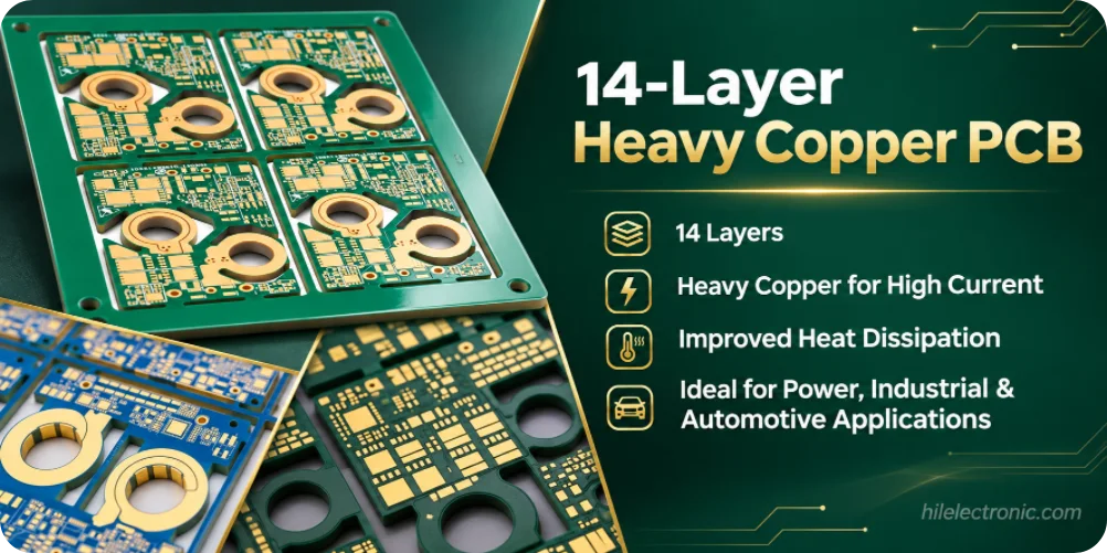
Mixed Copper Weight, Selective Heavy Copper and 14-Layer Stackup
A manufacturable stackup must account for the physical copper height and resin volume above each patterned layer. Heavy traces and planes leave deep channels between conductors that have to be filled during lamination without voids. Thick copper also demands larger etch compensation and clearance than a thin-foil signal layer. Copper weight needs to be specified as finished copper where relevant, not merely the starting foil label.
| 14-layer conductor choice | Ανησυχία για την κατασκευή | Απαίτηση σχεδίασης |
|---|---|---|
| Mixed copper weight | Etch clearance and resin flow differ by layer. | Finished copper specification for every layer. |
| Selective heavy copper | Thickness steps and transition geometry create local DFM checks. | Area map, step height and copper finish criteria. |
| High-current plated holes | Plating consistency and connection capacity require review. | Finished drill, hole copper and via array geometry. |
| Heavy copper and fine-pitch | Thick conductors and narrow lines may require separate layer solutions. | Layer-specific conductor/spacing rules and pad clearance. |
An asymmetrical distribution of copper can worsen bow and twist, particularly through multiple thermal cycles. The balance of core and prepreg, local copper density and sequence of lamination should be approved with the final board outline and connector requirements. For constructions with unusually thick inner planes, our multilayer PCB lamination service is a relevant engineering reference.
Can selective heavy copper and fine-line signals coexist on the same 14-layer PCB?
Potentially, with a suitable layout and process. Selective heavy copper, stepped copper or separate copper weights can preserve fine control routing while providing larger cross-sections where needed. However, the dimensions of a fine digital net cannot be assumed to remain identical after changing local copper plating or etching. Submit the complete copper map, finished thickness targets and required clearances for a manufacturing route review.
Heavy Copper DFM and Manufacturing File Review
Before fabrication, record the finished copper weight by layer and separate power nets from dense signal regions. Confirm minimum copper clearances, drill-to-copper gaps, intended hole wall thickness, board outline, insulation requirements and any selective plated area. A heavy-copper build can fail CAM review even when the nominal 14-layer count is routine, especially if narrow control traces were drawn with thin-copper etching rules.
The manufacturing process may need additional etch compensation, resin volume or a changed dielectric arrangement to meet the released requirements. Highleap’s Ανασκόπηση PCB DFM can flag these features. If the high-current design also uses blind/buried vias, the Διαδικασία κατασκευής PCB HDI needs an independent compatibility review rather than simply reusing an ordinary heavy-copper press schedule.
Can the fabrication supplier guarantee current capacity from a copper weight alone?
No. IPC-2152 provides engineering guidance relating conductor dimensions and temperature rise; final current capacity still depends on the complete product’s layout, cooling and operating conditions. The customer should provide current paths, maximum temperature rise and operating environment, while Highleap confirms the finished copper geometry and manufacturing evidence. For populated power boards, discuss a project-specific functional test scope if the test fixture and permissible load conditions are available.
Which information should be included with a high-current PCB drawing?
A project-ready drawing should include finished copper weight for every layer, net-specific current and voltage requirements, the allowable conductor temperature rise, hole current paths, copper-to-copper isolation, via structure, connector interface and the ambient/cooling conditions assumed in the thermal model. For designs with different copper weights on power and signal layers, identify any selective plating or step-copper features on separate fabrication layers, not only in a note saying “heavy copper.”
A supplier can review etch allowances and prepreg resin volume against the actual metal pattern. Where several vias distribute current between planes, require the via array, hole finish and plating criteria to be accepted as a system. An isolated statement such as “4 oz copper handles 20 A” would be misleading because trace width, temperature and heat transfer strongly affect current capacity.
Copper Weight, Current Capacity and Thermal Management

Current capacity is not determined by copper weight alone. Trace cross-section, length, permitted temperature rise, conductor surroundings, adjacent planes and heat removal all affect the result. A 4 oz trace of one width and length does not have a universal ampere rating that can be copied onto a different board. The OEM should supply the current and temperature requirements, along with any applicable thermal analysis and derating policy.
Highleap can evaluate power planes, parallel copper paths, thermal via arrays and local heat spreading against the existing stack. If a design also needs a mechanical heat spreader or a metal insert, the exact part geometry and process route must be confirmed separately; embedding copper coins or blocks should never be implied as standard on every fourteen-layer heavy copper build.
Does 10 oz copper automatically make a fourteen-layer board suitable for an EV inverter?
No. EV and industrial power assemblies depend on insulation coordination, continuous and transient current, temperature cycling, creepage/clearance, connector design, switching transients, fault protection and enclosure cooling. Highleap can manufacture a specified board construction, but the current rating and end-product safety approvals belong to the full design and its qualification plan. The factory’s published 10 oz copper ceiling is not an equipment-level inverter certification.
Plated Holes, High-Current Connections and Electrical Clearance
Heavy power planes may need reliable high-current transitions through plated barrels or carefully designed via arrays. The plated-hole wall thickness, available pad diameter, finished drill, aspect ratio and clearance from neighboring power domains should be designed as one system. A thick finished PCB with small holes has more demanding plating requirements than a thin board, even if the copper weight elsewhere is unchanged.
For press-fit power or signal connectors, specify the component manufacturer’s finished plated-hole window and insertion procedure. Highleap’s rigid capability page publishes a general press-fit tolerance, but the tolerance for the particular board should follow its thickness, plating and hole condition, as well as the connector system. If the layout includes selective edge plating, terminals or special slots, include a separate mechanical/finish drawing.
Should power interconnects use one large plated hole or several smaller vias?
The answer follows current density, available copper area, soldering/press-fit constraints, plating capability, manufacturing yield and thermal behavior. Via arrays distribute current and heat differently from one connector barrel, and they can also influence electrical isolation spacing. The design authority must establish the required current path; fabrication confirms the manufacturable finished hole geometry and inspection method.
Heavy Copper PCB Applications and Assembly

Fourteen-layer heavy copper builds can be specified for solar inverter control and interface boards, wind turbine power-control electronics, EV charging equipment, battery energy storage systems, motor drives, power distribution modules and high-current industrial control. The fourteen-layer construction allows control signals, protection functions, isolated measurement circuits and high-current copper to coexist when the electrical and manufacturing design permits.
Not every high-power product needs a fourteen-layer heavy copper PCB. A separate power substrate, a busbar and a multilayer controller may be more appropriate when switching currents or thermal loads are extreme. Highleap can coordinate related power-electronics PCB fabrication within a broader OEM board set; the customer’s system architecture determines which functions belong on this board and which should remain separate.
Heavy Copper PCB Assembly and High-Thermal-Mass Soldering
Assembling a fourteen-layer heavy copper board can require special attention to heat distribution, large terminals and high thermal mass. SMT solder profiles, power connector attachment, selective soldering and post-assembly electrical checks should be planned with the fabrication process. A generic reflow profile for a small two-layer FR-4 board is not automatically suitable for thick power copper and large components.
Highleap's Υπηρεσίες συναρμολόγησης PCB και ενσωμάτωσης εξαρτημάτων can be coordinated with the bare-board build. Depending on the design, the quotation can include BGA/QFN logic devices, through-hole power terminals, conformal coating and functional testing. The test plan should state load and isolation conditions, fixture design and operator safety; a PCB fabricator’s electrical netlist test is not a powered load test.
Quality Control, Microsections and Thermal Reliability
Inspection requirements may include internal copper imaging and registration checks, lamination integrity, hole-wall plating, minimum remaining clearances, board thickness, isolation/continuity testing and microsections of selected power and via features. For critical assemblies, define thermal-stress or other qualification sampling and the test coupons before production. A copper layer that passes a simple netlist test can still be unacceptable if its cross-section or insulation gap is out of drawing tolerance.
Use the specified IPC-6012 rigid-board performance class, applicable workmanship criteria and any customer-specific power reliability requirements. A production report should be traceable to the actual material/copper stack and fabricated lot. Conductor current-carrying performance is not established by IPC bare-board workmanship inspection alone and must be validated by the electrical/thermal design.
Can Highleap supply cross-sections for a high-current fourteen-layer PCB?
Cross-section preparation and documentation can be quoted as a project-defined acceptance deliverable, with coupon locations, inspected features, sample quantity and reporting format agreed in advance. Cross-sections can verify sampled plating or interface geometry; they do not establish the thermal rating of the entire populated power system. Request both the structural test and the separate electrical or environmental qualification evidence relevant to the product.
Lead Time, Cost and Material Planning
Cost depends on copper mass and distribution, laminate and prepreg, inner-layer etching, lamination fill, drilling/plating, finish, board dimensions, quantity and the contracted inspection evidence. A 14-layer construction with selective heavy copper may cost less than applying thick copper to all layers, but the routing and isolation design must remain compliant. A low-loss controller and a heavy power plane may also require a hybrid material or different copper profiles that increase manufacturing complexity.
For general high-layer price factors, the PCB fabrication cost and quotation guide distinguishes build features and test scope, while backplane PCB fabrication guidance addresses a different case where high-current planes must also support press-fit connectors and longer signal channels. On repeat programs, state the production forecast, approved materials, substitution restrictions and acceptance records so a prototype pricing assumption does not unexpectedly change when orders scale.
Request a 14-Layer Heavy Copper PCB Quote
Send Gerber/ODB++ artwork, the exact 14-layer order, finished copper weights by layer, stackup thickness, drill chart, isolation/clearance rules, current and thermal requirements, connector drawings, surface finish, quantity, quality class and requested acceptance data. If there is selective thick copper or a local power insert, attach a clearly dimensioned construction drawing with the intended final copper profile.
Highleap can review the combination of high-current routing, material choice, plating, insulation and board-level assembly, then propose a build-specific quotation with explicit assumptions rather than a universal price based only on ounces of copper.

συνιστάται Δημοσιεύσεις
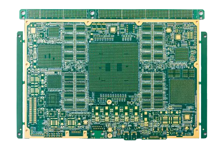
Κατασκευαστής PCB 14 στρώσεων στην Κίνα
ΠΡΟΣΑΡΜΟΣΜΕΝΗ ΑΚΑΜΠΤΗ ΠΟΛΥΣΤΡΩΜΑΤΙΚΗ ΠΛΑΚΕΤΑ Highleap Electronics...
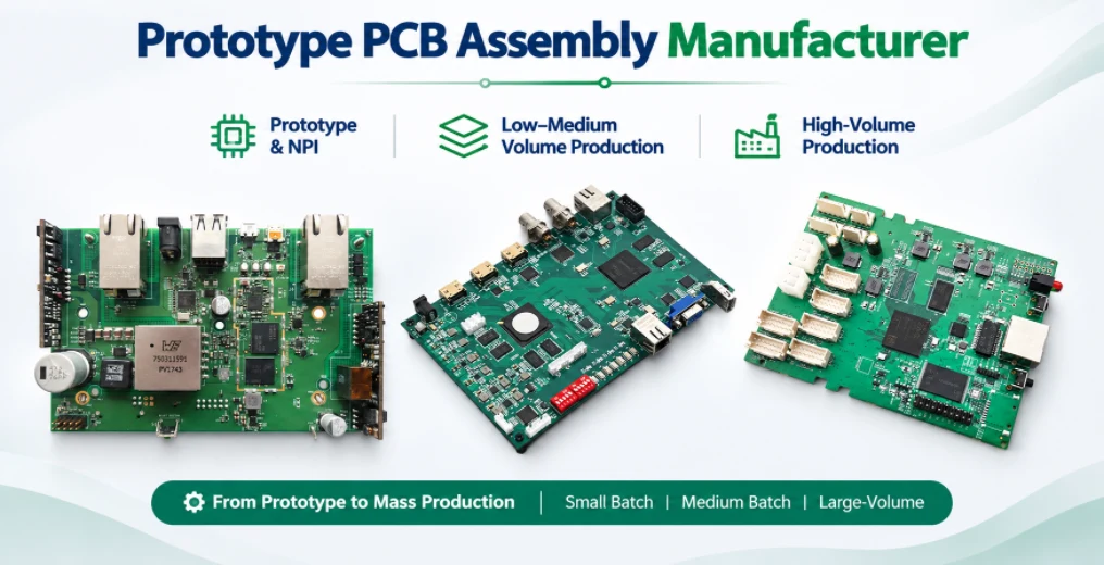
Συναρμολόγηση PCB 14 στρώσεων και κατασκευή PCB σε μία μόνο στάση
ΚΑΤΑΣΚΕΥΗ PCB + PCBA Η Highleap Electronics παρέχει 14...
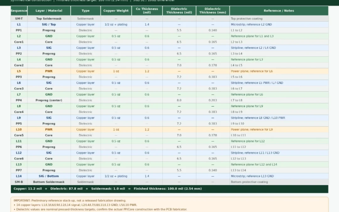
Στοίβαξη PCB 14 στρώσεων για κατασκευή υψηλής ταχύτητας και πολλαπλών στρώσεων
ΑΞΙΟΛΟΓΗΣΗ ΜΗΧΑΝΙΚΗΣ & ΣΤΟΙΒΑΖΕΩΣ Μια στοίβαξη PCB 14 στρώσεων είναι...
Κατασκευή πρωτοτύπων PCB 14 στρώσεων, χρόνος παράδοσης και επιθεώρηση
ΠΑΡΑΓΩΓΗ NPI / ΠΡΩΤΟΤΥΠΟΥΈνα πρωτότυπο PCB 14 στρώσεων θα πρέπει...
Πώς να λάβετε προσφορά για πλακέτες τυπωμένων κυκλωμάτων (PCB)
Ας εκτελέσουμε ανάλυση DFM/DFA για εσάς και ας επικοινωνήσουμε μαζί σας με μια αναφορά. Μπορείτε να ανεβάσετε τα αρχεία σας με ασφάλεια μέσω του ιστότοπού μας. Χρειαζόμαστε τις ακόλουθες πληροφορίες για να σας δώσουμε μια προσφορά:
-
- Gerber, ODB++ ή .pcb, spec.
- Λίστα BOM εάν χρειάζεστε συναρμολόγηση
- Ποσοτητα
- Χρόνος στροφής
Εκτός από την κατασκευή PCB, προσφέρουμε μια ολοκληρωμένη γκάμα ηλεκτρονικών υπηρεσιών, όπως σχεδιασμό PCB, PCBA και ολοκληρωμένες λύσεις. Είτε χρειάζεστε βοήθεια με την πρωτοτυποποίηση, την επαλήθευση σχεδιασμού, την προμήθεια εξαρτημάτων είτε τη μαζική παραγωγή, παρέχουμε ολοκληρωμένη υποστήριξη για να διασφαλίσουμε την επιτυχία του έργου σας.
Για υπηρεσίες PCBA, παρακαλούμε να μας δώσετε τον Πίνακα Υλικών (BOM) και τυχόν συγκεκριμένες οδηγίες συναρμολόγησης. Προσφέρουμε επίσης ανάλυση DFM/DFA για τη βελτιστοποίηση των σχεδίων σας για κατασκευασιμότητα και συναρμολόγηση, διασφαλίζοντας μια ομαλή διαδικασία παραγωγής.