
HIGHLEAP ELECTRONICS / BACKPLANES / PRESS-FIT INTERFACES
14 geruzako atzeko planoko PCB fabrikatzailea Txinan, prentsatzeko muntaketarako
Highleap Electronics provides custom 14 layer backplane PCB manufacturing in China for networking chassis, telecom equipment, industrial rack systems and modular electronics. A fourteen-layer backplane can combine controlled-impedance signal channels, distribution planes and dense connector fields when the board’s physical thickness, hole plating, registration and channel loss are engineered together. Highleap reviews the released backplane drawing and can coordinate connector installation or other specified PCBA operations as part of an OEM manufacturing program.
Backplane manufacturing starts with the mechanical and connector definition: daughter-card pitch, connector manufacturer, finished plated-hole window, chassis mounting points, maximum board size and operating interfaces. The physical stackup and drills are approved against those requirements. Our broader backplane PCB fabrication service describes related board families; this page addresses a specific fourteen-layer configuration and the deliverables required to fabricate it consistently.
Plan Your 14-Layer Backplane PCB
Send your stackup, connector drawings, press-fit hole requirements, backdrilling notes and quantity.
Konektorearen aztarna
Press-fit hole geometry, alignment and mating-card tolerances.
Taularen arkitektura
Power and return-plane design across many interface positions.
Signal channel
Loss, impedance and via stub geometry through backplane links.
Arakatu fabrikazio gida hau
BACKPLANE / PRESS-FIT CONNECTORS / 01
14-Layer Backplane PCB Capabilities and Applications

Backplane examples illustrate connector-dense board constructions; the ordered layer count is defined in the fabrication data.
Highleap-en PCB zurrunaren gaitasun-taula lists large-format multilayer manufacturing, controlled impedance, press-fit hole tolerance and advanced drilling capabilities. A project-specific backplane review determines whether the requested combination of outline size, panel yield, finished thickness, connector density and via aspect ratio is manufacturable. A published maximum board size or aspect ratio is not a guarantee that every large and densely drilled backplane can be released without changes.
The fabrication output can include bare-board electrical testing, dimensional inspection and contracted impedance or plating evidence. Highleap can also coordinate approved connector installation and functional checks, subject to fixture, force and test-plan requirements. For a full chassis project, separate line items may be needed for power harnesses, front-panel hardware and finished system integration.
Can a 14-layer backplane be manufactured with press-fit connectors?
Yes, the design can be reviewed for finished hole and plating specifications provided by the connector manufacturer. The PCB’s drill, copper deposition, hole-wall thickness, solder finish, allowable insertion force and board support must match the actual connector family. A broad tolerance claim from a capability table does not replace the connector drawing or a qualified press-fit process for the nominated order.
A backplane is not defined by fourteen layers alone: the connector architecture, board outline, rail distribution and chassis support govern the product. For a board that uses ordinary multilayer routing without backplane-specific connector requirements, the general 14 layer PCB manufacturing scope may be the more appropriate fabrication reference.
Server, Network Switch and Industrial Backplane Configurations
Fourteen-layer backplanes may be used in Ethernet switching shelves, industrial rack controllers, data-acquisition chassis, communication equipment and other modular platforms. A server-related design can need high-speed interfaces, a management bus and power distribution in one board; an industrial backplane may instead emphasize robust daughter-card insertion, analog isolation and easy maintenance.
Network / telecom
High-speed modular line-card and switching chassis.
Server / storage
Compute and storage interface backplanes with dense connectors.
Industrial / controls
Long-lived modular racks and equipment with robust connectors.
ATCA, CompactPCI, VME/VME64x, VPX and other standards describe different system and connector ecosystems. A PCB simply having fourteen layers does not make it compliant with any of them. Where a customer follows a named platform specification, Highleap requires the relevant outline, slot pitch, connector footprints, keep-outs, mechanical tolerances and electrical acceptance requirements to quote the exact implementation.
Does every 14-layer backplane need HDI microvias?
No. Dense connectors can often be served by mechanically drilled plated through-holes and careful layer allocation. HDI or blind/buried structures are justified when routing congestion or a specific connector escapes cannot be solved by a conventional fourteen-layer build. The selected interconnect route must be documented separately from the press-fit plated-hole requirements; the two hole types have different manufacturing and inspection needs.
BACKPLANE / PRESS-FIT CONNECTORS / 02
Stackup, Signal Integrity and Power Distribution

Connector examples; hole geometry and press-fit requirements must follow the selected connector specification.
A backplane stackup must maintain suitable reference planes and power distribution while supporting long signal runs and the required connector transitions. The released design should identify controlled-impedance net classes, reference layers, via stubs, laminate materials and maximum physical thickness. High-Tg, Dk and Df are not interchangeable material properties: a high-Tg grade may be appropriate for repeated assembly heat but insufficient for the permitted insertion-loss budget.
Low-loss channel
Confirm dielectric grade, copper profile and route length budget.
Layer reference
Define consistent return paths and transitions at each connector zone.
Egiaztapen elektrikoa
Specify impedance coupon evidence and optional loss measurements.
Power-plane layout
Separate return, supply, signal integrity and connector current requirements.
Highleap can review approved low-loss material families and hybrid constructions through its high-layer-count laminate service; the related Abiadura handiko PCB fabrikazio gida addresses channel-loss and controlled-coupon details when those are the principal constraints. The exact material grade, core/prepreg selection, glass style and copper profile should be included in the engineering release. A named MEGTRON, Isola or other brand is not a substitute for the specific material series and laminate data; material procurement and substitution must be agreed before fabrication.
Can a 14-layer backplane support 25G, 56G or 112G interfaces?
The PCB can be engineered toward a defined channel specification, but no data rate follows automatically from its layer count or laminate brand. End-to-end loss, reflections, crosstalk, connectors, board length and active-device equalization govern the link. Highleap can fabricate and inspect the approved physical stack and agreed coupons; system-level link compliance needs the customer’s full channel and test criteria.
Power Distribution, Ground Planes and Mixed Copper Weights
A fourteen-layer backplane may deliver several voltage domains alongside control and communication signals. Continuous ground references, power-plane splits, connector pin assignments and the necessary copper cross-section must be coordinated to avoid return-current discontinuities or excessive voltage drop. Heavy or mixed copper may be suitable for specific power layers, but the entire fourteen-layer stack need not be heavy copper.
When high-current distribution is substantial, assess whether a separate busbar or power module is more appropriate than adding excessive copper to every signal layer. Highleap’s heavy copper PCB manufacturing guidance is relevant when power-plane copper and resin filling drive the design, while the broader heavy copper PCB service covers other multilayer constructions. The final current rating remains a product-level electrical and thermal design result.
BACKPLANE / PRESS-FIT CONNECTORS / 03
Press-Fit Holes, Backdrilling and Mechanical Tolerances
Connector-hole quality is a primary backplane manufacturing requirement. The receiving board must maintain finished hole diameter, plating thickness, hole position and board flatness within the connector maker’s operating window. Poor registration can reduce annular ring or create misalignment across long connector rows. The board drawing should specify datum references and hole-by-hole special tolerances rather than relying on one global note.
| Press-fit feature | Engineering data to supply | Quality evidence to agree |
|---|---|---|
| Connector manufacturer & series | Part number, drawing revision, compliant pin specification. | Material/part traceability and approved interface. |
| Finished PTH diameter | Hole tolerance, barrel condition and plating definition. | Hole measurement and sample cross-section if required. |
| Connector grid | True-position datum, insertion sequence and board support. | Mechanical fit, insertion procedure and fixture confirmation. |
| Repair / rework limits | Replacement rules, mating cycles and concession ownership. | Inspection after any permitted rework. |
The mechanical drawing should distinguish plated press-fit holes, ordinary plated vias, non-plated tooling holes, slots and mounting features. For a large connector field, tolerance stack-up between daughter-card guides, chassis datum and PCB outline can be as important as individual hole diameter. A press-fit insertion tool requires a support fixture and a defined insertion force; bare-board inspection by itself cannot verify that the final connector assembly was installed correctly.
What documentation is needed for press-fit connector approval?
Supply the actual connector part number and manufacturer’s plated-hole specification, press-fit force/displacement instructions, permitted board thickness and support-fixture requirements. Ask for the agreed plated-hole measurement method and sample plan. If the system requires monitoring insertion force or post-install continuity, identify those records as assembly deliverables before ordering.
Backdrilling, Via Stubs and Differential Signal Routing
On a fourteen-layer board with long multi-gigabit channels, an unused plated-through-hole stub may degrade return loss. Backdrilling is selective, applied to designed transitions where the residual barrel matters; it should not be ordered indiscriminately on every via. The backdrill map needs drill side, depth, stub specification, active copper clearances and an appropriate inspection method.
Highleap-en backdrilled PCB fabrication process addresses the mechanical operation. The channel design should also control return paths, discontinuities at connectors and pair-to-pair skew, rather than expecting backdrilling alone to compensate for all signal-integrity problems. Differential impedance coupon tests are not the same as full-channel S-parameter or live system validation.
Can press-fit holes also be backdrilled?
The combination requires a specific engineering review. Connector contact zones, plated barrel length and hole integrity must not be compromised by a depth-controlled drill operation. If the signal pin uses a press-fit interface and an associated stub is electrically significant, the connector manufacturer and PCB fabricator should agree the permissible backdrill strategy before release.
Large-Format PCB Thickness, Warpage and Mechanical Fixtures
Backplane dimensions and connector count can make manufacturing handling a critical factor. A larger panel is more sensitive to layer registration, board warp and tooling support. The actual board thickness should follow both impedance construction and connector requirements; arbitrarily thickening the board can worsen the aspect ratio of small holes and create difficult drilling or plating conditions.
Outline & slot grid
Agree chassis datums, stiffeners, board size and keep-outs.
fabrikazio
Lock layer order, copper balance, press-fit pattern and backdrill.
Konektorea sartzea
Agree fixture, force range and non-damaging support.
Chassis test
Confirm mating cards, system interface and any customer functional checks.
If the finished board requires stiffeners, support rails or special chassis brackets, supply the 3D mechanical model or approved drawings. The fabrication quality plan should state outline/slot tolerances, mounting-hole datums, board thickness and any bow/twist limit under a defined measurement condition. Assembly procedures should avoid applying connector insertion loads without adequate support.
How should a 14-layer backplane production release define connector interfaces?
List the connector manufacturer and complete part number, mating daughter-card geometry, connector insertion plan, finished press-fit hole tolerances, plating thickness and hole-wall condition. An approved connector drawing may have tighter requirements than a generic PCB PTH drawing. Manufacturing review should compare the connector specification with the selected multilayer thickness and copper patterns around the holes. The customer should approve fixture access and any insertion-force or retention test before the first production batch.
For high-speed backplanes, include the differential impedance matrix and the via transition drawings associated with each connector zone. Do not treat the connector’s nominal data-rate designation as a guarantee of board-level insertion loss; the laminate, route length, via stub and full channel interfaces still need an electrical budget and an appropriate verification plan.
Validate Your Backplane Connector Requirements
Submit the connector drawings, board outline, press-fit tolerances and channel requirements.
BACKPLANE / PRESS-FIT CONNECTORS / 04
Backplane Testing, Quality Control and Traceability

A populated backplane example with multiple connector rows.
A backplane acceptance plan should include the approved netlist, finished dimensions, selected connector-hole measurements, drilling/plating inspection, electrical continuity/isolation testing and any specified impedance coupons. The manufacturing stage can verify bare-board properties; after connector installation, insertion-force checks, contact continuity, link testing and mechanical fit become separate assembly or system-level tasks.
Bare-board continuity / isolation
Netlist electrical acceptance of fabricated board.
Press-fit hole inspection
Dimensional / plating condition relevant to connector pin system.
Signal channel evidence
Coupon impedance and optional defined channel metrics.
First-article chassis fit
Alignment, bow/twist and mating geometry to customer drawing.
The applicable IPC-6012 rigid-board performance class should be stated on the fabrication order, with relevant IPC-A-600 workmanship criteria and any additional customer-specific requirements. A microsection or other destructive test requires a sampling plan, location and acceptance criterion. For a backplane with sensitive link channels, request the exact impedance or loss evidence needed rather than assuming a generic “100% test” proves system throughput.
What should a backplane first-article report include?
The report can identify board part/revision, approved laminate and stackup, finished dimensions and thickness, critical press-fit holes, plating and netlist results, contracted coupons and any recorded deviations. If installed connectors are included in the order, a separate assembly inspection should cover part identity, position, insertion process and agreed electrical checks. This keeps bare-board conformance distinguishable from finished chassis functionality.
Backplane Supplier Qualification, Production Transfer and Lot Traceability
A backplane production program should keep the connector part numbers, fabrication data, physical stackup, press-fit hole requirements, test coupons and chassis revision under common configuration control. Repeated orders must preserve the approved laminate and copper structure; if board size, material grade or production tooling changes, the impact on flatness and mechanical alignment must be assessed before release. A qualified bare board is not automatically a qualified connector assembly.
Supplier-review evidence can include a clearly identified production site, the applicable certificate scope, a sample inspection report, a manufacturing route and an agreed deviation/repair policy. For a transfer from an existing assembler, Highleap can review the current artwork, connector installation work instructions, known field returns and fixtures through its PCB assembly production-transfer support.
Can a 14-layer backplane be supplied as a fully assembled chassis module?
Highleap can evaluate the PCB, installed connectors and other turnkey assembly requirements as separate deliverables. A complete chassis may require mechanical assembly, wire harnesses, daughter-card installation, firmware and powered interface tests; these need their own BOM, fixtures, instructions and acceptance evidence. An assembled backplane with inspected connectors should not be represented as a completely qualified server or telecom system without the corresponding system tests.
BACKPLANE / PRESS-FIT CONNECTORS / 05
Backplane PCB Assembly and Chassis Integration
Highleap can coordinate a fourteen-layer bare backplane with approved connectors, selective SMT components, mechanical hardware and defined tests. Press-fit installation requires the correct tooling and board support; wave or selective soldering requirements differ from mechanical insertion, and neither should be assumed to be included without a defined assembly drawing. The PCB muntaketa zerbitzuak provide the corresponding manufacturing scope.
For modular systems, a finished-unit quote may also cover card guides, panel parts, power harnesses and packing. Electrical validation should identify what is checked on the bare backplane, after connector installation and after the assembled daughter cards are fitted. Any claimed 25G or 100G system qualification must be linked to the actual contracted fixture, test conditions and results.
BACKPLANE / PRESS-FIT CONNECTORS / 06
Request a 14-Layer Backplane PCB Quote
Submit Gerber/ODB++/IPC-2581, the exact fourteen-layer map, approved laminate or alternatives, finished thickness, board and chassis outline, connector part numbers, plated-hole and backdrill drawings, target impedance/loss requirements, copper weight by layer, quality class and quantities. If connector insertion or chassis-level assembly is required, add mechanical models, BOM, assembly drawings, insertion/test fixture details and defined pass/fail criteria.
Highleap can review the proposed physical construction, manufacturing/assembly split, test evidence and project schedule, then return an RFQ response based on the complete backplane rather than only the layer count and outline size.
Request Custom 14 Layer Backplane PCB Manufacturing
Bidali taularen marrazkia, ezaugarri bereziak, nahi diren materialak eta eskaera-bolumenak. Highleap-ek fabrikazio-bideragarritasuna, ikuskapen-eremua eta aukerako muntaketa berrikusi ditzake aurrekontu sendoa eman aurretik.

Gomendatzen Mezuak

OEM prototipoetarako eta ekoizpenerako alumina PCB fabrikazioa
HIGHLEAP ELECTRONICS · Alumina Zeramikazko PCB Fabrikazioa...

OEM eta ODM elektronika fabrikaziorako PCB muntaketa hornitzailea
HIGHLEAP ELECTRONICS · OEM / ODM PCB Muntaketa HornitzaileaZure...
Al2O3 zeramikazko PCB fabrikatzailea zehaztasun zeramikozko zirkuituetarako
HIGHLEAP ELECTRONICS · Aluminio Oxidozko Zirkuitu Zeramiko...
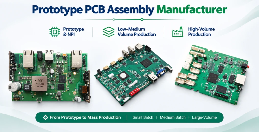
Prototipo PCB Muntaketa Fabrikatzailea
Highleap Electronics PCB muntaketa prototipo bat da...
Nola lortu aurrekontua PCBetarako
Egin dezagun DFM/DFA analisi bat zuretzat eta txosten batekin erantzungo dizugu. Zure fitxategiak modu seguruan igo ditzakezu gure webgunearen bidez. Aurrekontua emateko, honako informazio hau behar dugu:
-
- Gerber, ODB++ edo .pcb, zehaztapenak.
- BOM zerrenda muntaia behar baduzu
- Kopurua
- Piztu ordua
PCB fabrikazioaz gain, zerbitzu elektroniko sorta zabala eskaintzen dugu, besteak beste, PCB diseinua, PCBA eta giltza eskurako irtenbideak. Prototipoak egiteko, diseinuaren egiaztapenerako, osagaien hornikuntzarako edo ekoizpen masiborako laguntza behar baduzu, zure proiektuaren arrakasta bermatzeko laguntza osoa eskaintzen dugu.
PCBA zerbitzuetarako, eman zure BOM (Materialen Zerrenda) eta muntaketa-argibide espezifikoak. DFM/DFA analisia ere eskaintzen dugu zure diseinuak fabrikazio eta muntaketa optimizatzeko, ekoizpen-prozesu leuna bermatuz.