
FPGA Mechanical Keyboard PCB Manufacturing and Assembly
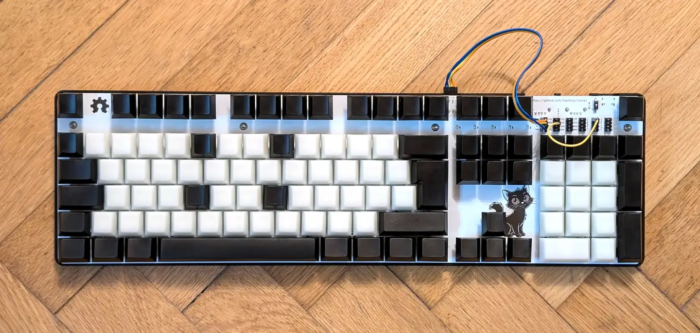
Figure 1. Assembled Clavier reference keyboard. This is an open-source project photograph, not a Highleap customer product or factory build. Image: lsartory / Clavier, CC BY 4.0; resized and converted to WebP.
A mechanical keyboard with an FPGA and an integrated USB hub is not a routine switch-board assembly. Its production success depends on the coordination of a multi-layer PCB, fine-pitch component placement, BGA solder-joint quality, USB connectivity, programming access and repeatable functional tests. A design can look complete in CAD and still create production risk if its stack-up, assembly data, test access or mechanical interfaces are not released clearly.
This engineering case study uses Klavye, an open-source full-size FPGA-based mechanical keyboard listed in the help-14 mechanical keyboard project index. The repository documents a 105-key ISO layout plus one extra key, Cherry MX PCB-mounted switch compatibility, N-key rollover, a stated 1000 Hz polling rate, a two-port USB 2.0 hub and JTAG, SPI, I²C, UART and GPIO interfaces. It also publishes a four-layer PCB and identifies 0402 passives and an FPGA in BGA packaging as the main reasons hand assembly is difficult.
İçindekiler
- What the Clavier Reference Design Tells a PCB Manufacturer
- Mechanical Keyboard PCB Manufacturing with Two Layer and Four Layer Designs
- BGA and 0402 Assembly Need a Process Plan Before the First Build
- USB Hub and Communication Interfaces Must Be Testable
- Mechanical Integration Is Part of PCB Manufacturing Readiness
- Release a Complete Manufacturing Data Package
- Define Functional Testing Before the PCB Is Assembled
- How Highleap Electronics Can Support Keyboard PCB and PCBA Projects
- Sıkça Sorulan Sorular
The purpose of this article is not to present the Clavier design as a Highleap product. It is to show the engineering checks that matter when a keyboard developer moves from an open hardware reference or prototype to a controlled PCB fabrication and PCBA order. The same review logic is useful for other custom keyboards that combine dense switch layouts, programmable logic, fine-pitch ICs and USB peripherals.
1. What the Clavier Reference Design Tells a PCB Manufacturer
The Clavier repository is useful because it provides more than a finished-keyboard photograph. It includes a KiCad PCB project, a schematic PDF, housing design files and images of the assembled keyboard and programming interface. The repository also identifies separate licenses for the hardware, FPGA code and photographs.
| Yayınlanan proje detayları | Üretimle ilgili | What must be confirmed for a production order |
|---|---|---|
| 105-key ISO layout plus one extra key | Large board outline and many switch positions | Board dimensions, switch footprint, stabilizer and plate alignment |
| PCB-mounted Cherry MX switch compatibility | Switch-hole and pad geometry affect mechanical fit and soldering | Exact switch model, footprint revision and plate tolerance |
| Dört katmanlı PCB | Requires a controlled layer stack and CAM review | Finished thickness, copper weights, dielectric construction and any impedance targets |
| FPGA in BGA packaging and 0402 passives | Fine-pitch SMT assembly and hidden-joint inspection planning | Exact FPGA MPN, package drawing, land pattern, stencil and inspection criteria |
| Two-port USB 2.0 hub | Connector, routing, power and downstream-port validation | Hub IC, port configuration, protection, current limits and required USB operating mode |
| JTAG, SPI, I²C, UART and GPIO | Programming and interface test access | Pin map, test points, programming procedure and pass/fail limits |
The project README says the PCB has four layers and does not require unusual fabrication capabilities, while noting that manual assembly is difficult because of 0402 passives and the BGA FPGA. This distinction matters: board fabrication complexity and assembly complexity are not the same thing. A four-layer board may be straightforward to fabricate for a capable multilayer supplier, yet still require a tightly controlled SMT process and suitable inspection for its component package mix.
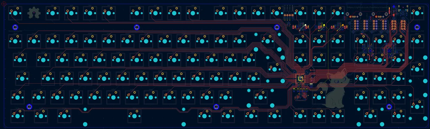
Figure 2. PCB layout image published in the Clavier repository. It is a project reference image, not the native manufacturing data and not a substitute for Gerber or ODB++ review. Image: lsartory / Clavier, CC BY 4.0; resized and converted to WebP.
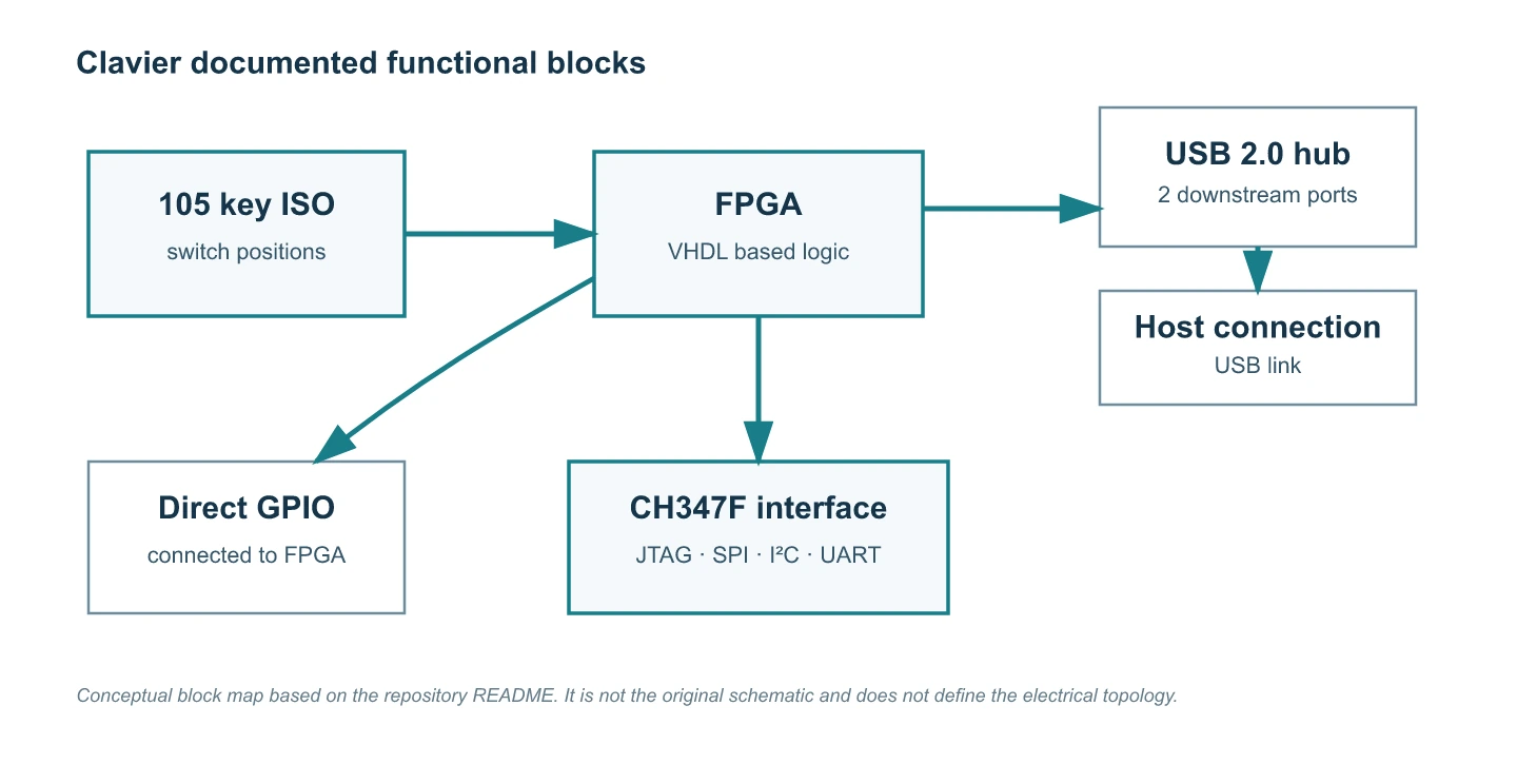
Figure 3. Conceptual block map based on functions described in the project README. It is not the original schematic and does not define the electrical topology or net connections.
2. Mechanical Keyboard PCB Manufacturing with Two Layer and Four Layer Designs
For many wired mechanical keyboards, a two-layer FR-4 PCB is a practical starting point. A conventional key matrix, diodes, a suitable microcontroller and USB connectivity can often be implemented with two copper layers when the routing and return paths are engineered correctly. Even some hot-swap and RGB keyboard designs use two-layer boards. Adding layers does not automatically improve a keyboard, and specifying four layers without an electrical or manufacturing reason may increase cost.
Açık kaynak Korne klavyesi family includes two-layer PCB implementations, making it a useful counterexample to the idea that mechanical keyboards require multilayer construction. Klavye, the FPGA project analyzed here, explicitly uses four layers. These are different design choices with different constraints, not conflicting manufacturing facts.
Why Two Layer PCB Fabrication Works for Many Mechanical Keyboards
A two-layer PCB has top and bottom copper separated by a dielectric core. For a keyboard whose MCU, key matrix and peripheral routing fit within two layers, this can be an economical solution for prototypes, pilot runs and production quantities. But routing completion alone is not a sufficient release criterion. Ground continuity, ESD protection, connector mechanical strength, LED power distribution, switch alignment and production-test access must also be reviewed.
Two-layer mechanical keyboard PCB DFM priorities include:
- Key switch geometry: confirm center positions, mounting holes, switch pin patterns and stabilizer cutouts with the selected switches, plate and housing, not just a screenshot of the layout.
- Hot-swap socket pads: check the exact footprint and mounting side, solder-mask openings, pad support and mechanical load during switch insertion and removal.
- Matrix routing and diodes: match row and column nets, diode orientation and test mapping to the approved schematic and firmware definition.
- Ground and USB routing: preserve suitable return paths and meet the selected USB controller’s routing and ESD requirements. USB High-Speed designs may require more stringent differential-pair controls than a basic full-speed keyboard.
- RGB and power: check LED count, power-rail voltage drop, trace capacity and available power; RGB by itself does not mandate a four-layer board.
- Üretim ve montaj: specify finished board thickness, copper weight, surface finish, drill details and solder-mask requirements. Confirm whether components and hot-swap sockets are assembled on one or both sides, and plan panelization accordingly.
When a Four Layer Keyboard PCB Makes Engineering Sense
A four-layer PCB may be justified when a dense device such as a BGA FPGA needs more routing space, when power and ground distribution cannot be implemented satisfactorily on two layers, or when complex connectors and interface routing benefit from dedicated reference planes. It is not required merely because the keyboard is premium, has lighting, or uses wireless connectivity. The decision should be based on the released electrical design and manufacturing constraints.
| Mühendislik faktörü | Two layer keyboard PCB | Four layer keyboard PCB |
|---|---|---|
| Genel Başvuru | Wired key matrices and many moderate-complexity designs | Some dense BGA, hub and mixed-interface designs |
| Routing and ground | Signals and ground must share the two outer layers | Additional copper layers can support routing and reference planes |
| Mekanik uyum | Switch, socket, plate and case alignment remains critical | Exactly the same mechanical checks still apply |
| Maliyet etkisi | Typically less expensive at equivalent size and specification | Typically more expensive due to added fabrication steps |
| Factory review | DRC, outline, drilled holes, mask, copper clearances and panelization | All basic checks plus stack-up, inner layers and any impedance requirements |
| Seçim kuralı | Use if routing and reliability requirements are met | Use only when the design has a specific need |
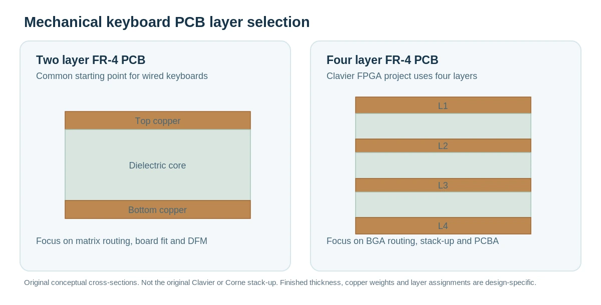
Figure 4. Original conceptual comparison of two-layer and four-layer keyboard PCBs. It is not the exact Clavier or Corne manufacturing stack-up.
Why the Clavier FPGA Keyboard Uses Four Layers
MKS Clavier project’s README belirtir four-layer PCB and identifies the BGA-packaged FPGA and 0402 passive components as reasons that manual assembly is difficult. This makes Clavier an advanced keyboard PCBA case study, not a specification that should be generalized to ordinary keyboards. Its README does not provide a complete fabrication stack-up, so the supplier should confirm the actual layer assignments, dielectric construction, copper weights, finished thickness and any controlled-impedance requirements from the approved files.
For this particular design, review FPGA breakout and via geometry, the USB 2.0 hub circuitry, ground and power connections, board outline, switch coordinates, connector locations, plated and non-plated drills, and enclosure alignment. Do not assume the hub operates at USB High-Speed merely because the project calls it USB 2.0; verify the actual interface requirements from the schematic and component datasheets.
For keyboard brands and hardware developers, the manufacturing principle is simple: start with the two-layer option if it meets the design requirements; choose four layers when the circuitry and layout justify it. For a project-specific quotation, send the PCB design files, fabrication notes, BOM, component placement data, target quantity and assembly requirements to Highleap Electronics keyboard PCB manufacturing and assembly. A proper DFM and PCBA review helps identify avoidable cost and assembly risks before production.
DESIGN REVIEW
Two layers or four for your keyboard PCB?
Share your layout or stack-up for a DFM review. Highleap can flag ground return paths, BGA fan-out and switch footprint issues before you commit to fabrication.
3. BGA and 0402 Assembly Need a Process Plan Before the First Build
The Clavier author specifically identifies the BGA FPGA and 0402 passive components as the main obstacles to easy hand assembly. For a PCBA supplier, these components call for a repeatable SMT process rather than an improvised manual build.
BGA package review
Before quoting or programming the assembly line, confirm the exact FPGA manufacturer part number and package code. The package drawing and PCB footprint must agree on ball pitch, ball map, orientation, land dimensions and any thermal or ground-pad requirements. The BOM should identify the exact orderable part, not only the FPGA family name.
The assembly plan should also define component moisture-sensitivity handling where applicable, solder-paste selection, stencil design, placement data, reflow profile development and the inspection method for hidden solder joints. X-ray inspection is commonly used to assess BGA joints that cannot be viewed directly; the inspection criteria should be agreed for the actual package and customer requirements.
0402 passive placement
For 0402 components, verify that the BOM package designation, footprint and manufacturer part number refer to the same physical size. Review polarity-sensitive parts, reference designators, pad geometry and clearance around the FPGA and other dense components. Stencil aperture design and solder-paste volume should be evaluated against the actual board layout and assembly process.
Reflow and post-reflow inspection
The reflow profile should be established for the selected solder paste, PCB thermal mass and component mix. Do not copy a profile from an unrelated board. AOI can help identify visible placement and soldering defects, while X-ray may be required for hidden BGA joints. Any rework method should be controlled so that nearby fine-pitch components and PCB pads are not damaged.
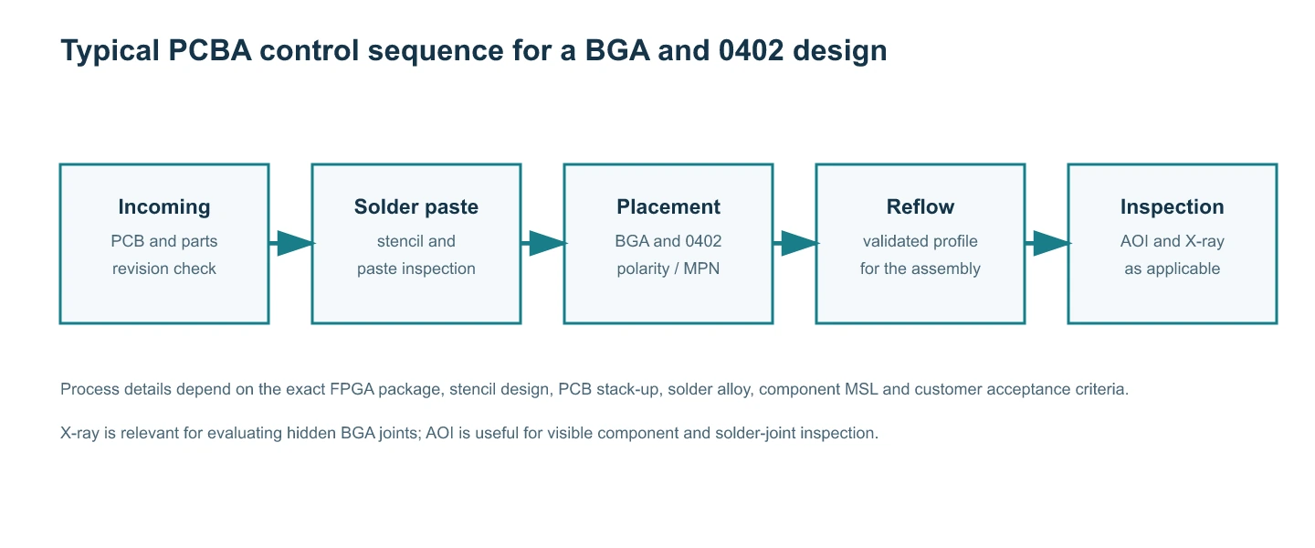
Figure 5. Typical process-control sequence for a BGA and 0402 assembly. Exact equipment settings and inspection criteria must be established for the released BOM and PCB revision.
4. USB Hub and Communication Interfaces Must Be Testable
The Clavier repository describes an integrated two-port USB 2.0 hub. It also states that the CH347F handles the communication interfaces JTAG, SPI, I²C and UART, while the GPIOs are connected directly to the FPGA.
For production, the design owner should provide the USB hub IC and connector part numbers, the intended host connection, downstream-port configuration, power requirements and any ESD or overcurrent protection requirements. The public README does not specify the exact USB speed mode, power budget or protection circuit, so these should be taken from the schematic and component datasheets rather than assumed.
The test plan should verify both downstream USB ports independently. A port that supplies power is not necessarily passing data correctly. Where the product specification requires data transfer, test enumeration and the required data function with a known-good host and test device.
For the auxiliary interfaces, define the JTAG programming procedure and identify how SPI, I²C, UART and GPIO functions will be exercised. Test pads, headers or fixture access should be designed into the product before the PCB is frozen. If programming access is hidden after enclosure assembly, the production sequence must account for that.
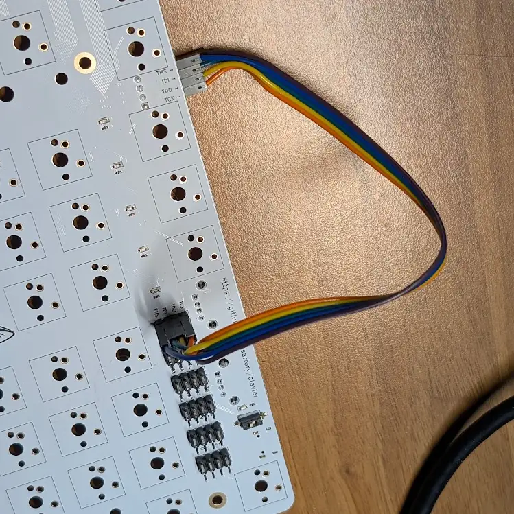
Figure 6. JTAG connection photograph from the Clavier project. The production fixture and programming procedure for a new product must be defined independently. Image: lsartory / Clavier, CC BY 4.0; resized and converted to WebP.
5. Mechanical Integration Is Part of PCB Manufacturing Readiness
The keyboard PCB is only one part of the mechanical assembly. The switch plate, housing, fasteners, keycap clearance, connector openings and PCB mounting features must agree with the electrical design.
The Clavier repository includes housing models and describes two housing versions. The second version changes the keyboard angle to 8 degrees to improve ergonomics. That is a useful reminder that mechanical revisions can affect connector access, board support, screw positions and the final fit even when the PCB itself has not changed.
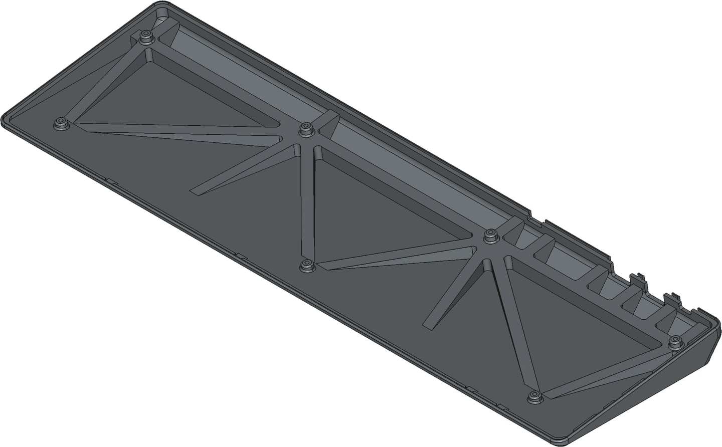
Figure 7. Housing render from the Clavier repository. Verify the current STEP model and the PCB revision together before releasing production data. Image: lsartory / Clavier, CC BY 4.0; resized and converted to WebP.
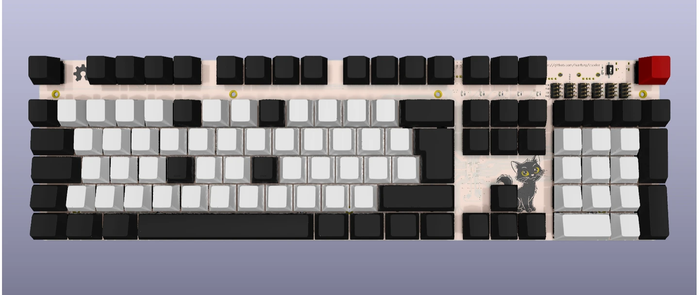
Figure 8. Clavier product render from the project repository. It illustrates the product layout; it is not a Highleap-manufactured product. Image: lsartory / Clavier, CC BY 4.0; resized and converted to WebP.
A practical mechanical review should include:
- PCB-to-plate alignment and switch center coordinates.
- Mounting-hole locations, screw access and standoff height.
- USB connector alignment with the enclosure opening.
- Component height and clearance under the housing.
- Board support near connectors and other mechanically loaded areas.
- Assembly order, access to programming points and serviceability.
Use the current STEP or equivalent 3D model where available. A 2D outline alone may not reveal interference between a BGA/connector component, the enclosure, fasteners or the plate.
6. Release a Complete Manufacturing Data Package
For a complex keyboard PCBA, a single Gerber archive is not enough. The manufacturing package should identify one controlled revision across PCB fabrication, assembly, firmware and mechanical documents.
| File or information | Amaç | Common issue if missing |
|---|---|---|
| Gerber X2 or ODB++ and NC drill | PCB fabrication and CAM review | Incomplete layers, ambiguous outline or drill definitions |
| İmalat çizimi ve katman düzeni | Layer construction, thickness, copper, finish and tolerances | Supplier assumptions about board construction |
| Üretici parça numaralarını içeren malzeme listesi (BOM). | Exact component sourcing and approved alternates | Wrong FPGA, package, passive value or unavailable part |
| CPL / centroid file | X/Y position, rotation, side and reference designator | Incorrect component orientation or placement side |
| Montaj çizimleri | Polarity, connector orientation, special assembly notes | Ambiguous top/bottom assembly or unmarked manual parts |
| Schematic and native design files | Connectivity review and engineering clarification | Limited ability to investigate net or footprint questions |
| FPGA image and JTAG instructions | Programming and bring-up | Board assembled but not configured or testable |
| Fonksiyonel test planı | Defines acceptance criteria and pass/fail limits | Subjective or incomplete final inspection |
| Mechanical STEP / DXF | Housing, plate, connector and mounting verification | PCB passes electrical checks but fails final assembly |
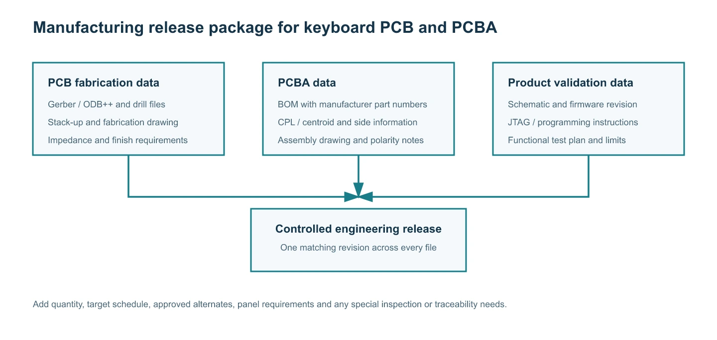
Figure 9. Manufacturing release package. The revision of the Gerber, BOM, CPL, assembly drawing, firmware and mechanical model should be consistent.
Before ordering, state the prototype or production quantity, required delivery window, approved component substitutions, panelization requirements, inspection expectations and any traceability requirements. If the FPGA or another key component is customer-supplied, identify that clearly in the BOM and quotation request.
7. Define Functional Testing Before the PCB Is Assembled
The Clavier README lists N-key rollover, a 1000 Hz polling rate and a two-port USB hub among its features. These are product-level claims that should be translated into measurable acceptance tests for the production version. A simple power-on check cannot prove that the keyboard behaves as specified.
| test alanı | Önerilen doğrulama | Kabul tanımı |
|---|---|---|
| Güç girişi | Check supply rails, polarity and current draw | Released voltage and current limits |
| FPGA programming | Program through JTAG and confirm expected configuration status | Approved image/version and successful readback or status check |
| Key scanning | Test every physical key position against the released key map | No missing, duplicated or incorrect key events |
| N-anahtar geçişi | Run defined simultaneous-key combinations | Specified combinations register correctly |
| Yoklama oranı | Measure with the agreed host and test method | Target and tolerance defined by product owner |
| USB hub | Test both downstream ports for power and required data function | Each port passes the product-specific test |
| JTAG and serial interfaces | Exercise JTAG, SPI, I²C and UART functions as applicable | Interface-specific test limits and pin map |
| Mekanik uyum | Check switch seating, connector alignment, plate and enclosure | Released mechanical drawing and fit criteria |
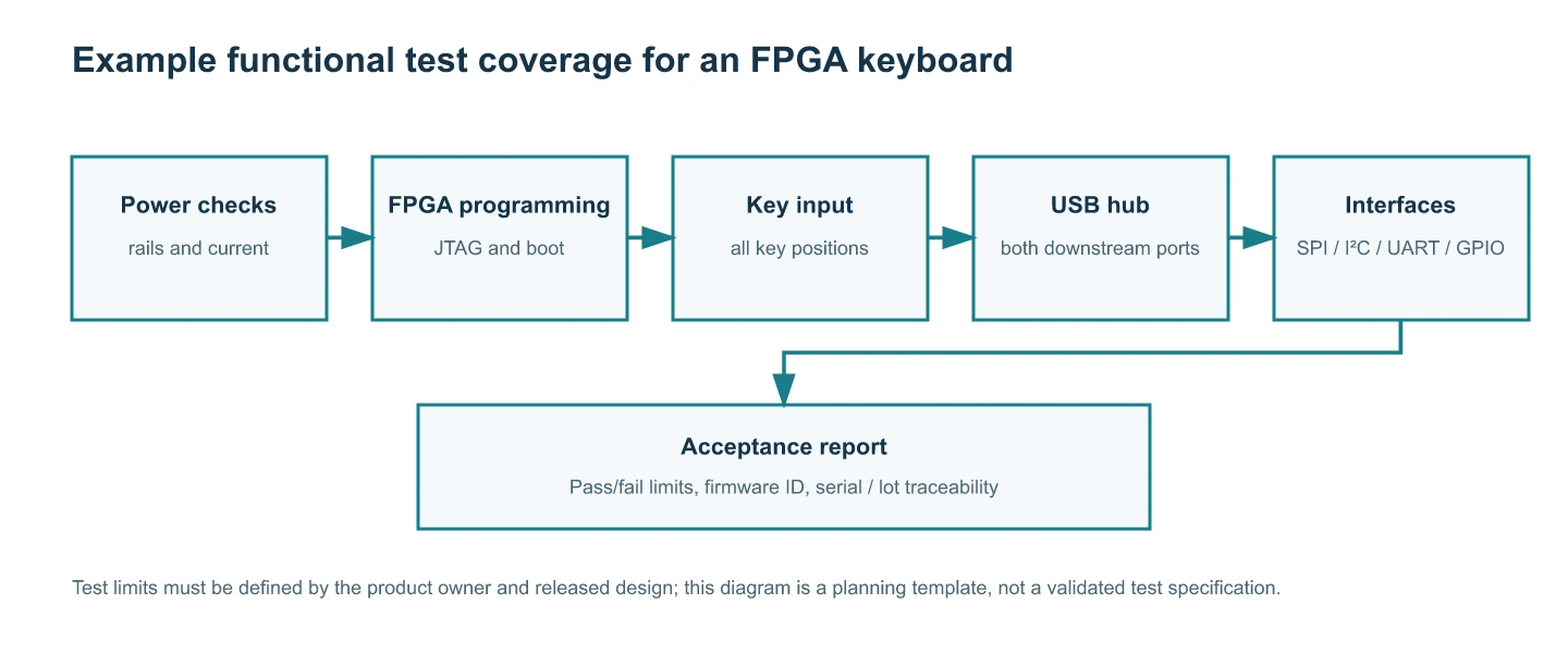
Figure 10. Example test coverage for an FPGA-based keyboard. The final test fixture and limits should be agreed with the product owner before the pilot build.
For a pilot build, capture failures by PCB revision, component lot and assembly batch. If a test fails, record whether the root cause is electrical design, component sourcing, assembly, firmware or mechanical integration. This makes engineering changes traceable and helps prevent the same defect from recurring in a later run.
8. How Highleap Electronics Can Support Keyboard PCB and PCBA Projects
Highleap Electronics provides PCB fabrication and PCB assembly services. Its published service information lists multilayer PCB fabrication, component sourcing, SMT and DIP assembly, AOI, X-ray inspection, electrical performance detection and functional testing. The PCBA page also lists 0201 as the smallest chip size and describes BGA assembly capabilities.
For a keyboard design with a four-layer board, BGA FPGA and 0402 passives, the practical next step is a project-specific engineering review. The exact FPGA package, pitch, board outline, stack-up, component list and required inspection method should be checked against the current production process before the order is confirmed.
- PCB üretim hizmetleri for multilayer board production and fabrication requirements.
- PCB montaj hizmetleri for component sourcing, SMT/DIP assembly and inspection options.
- Anahtar teslim PCB montajı for projects that need fabrication, sourcing, assembly and testing coordination.
- Keyboard PCB manufacturing and assembly for the dedicated keyboard service page.
PCB FABRICATION + ASSEMBLY
Get a Quote for Your Keyboard PCB and Assembly
Ready for prototypes or a production run? Send your design package for a project-specific quote covering board fabrication, component sourcing and assembly.
- Gerber or ODB++, NC drill and stack-up
- BOM, placement file and assembly drawings
- Target quantity, delivery date and test requirements
9. Sık Sorulan Sorular
Does a mechanical keyboard PCB need two layers or four layers?
Many conventional wired mechanical keyboards use two-layer FR-4 PCBs. A four-layer PCB may be justified by BGA fan-out, complex interfaces or ground and power constraints, but it is not the default for every keyboard. Clavier explicitly uses four layers because it is a specific FPGA-based reference design. The correct choice depends on DRC, CAM, DFM and the approved fabrication specification.
Why is BGA assembly important for an FPGA keyboard?
BGA solder joints are hidden beneath the package. The process therefore depends on the correct footprint, stencil, placement, reflow and inspection plan. X-ray inspection may be needed to evaluate hidden joints, depending on the package and customer requirements.
What files are needed for a keyboard PCBA quotation?
Provide Gerber or ODB++, drill files, fabrication drawing, BOM with manufacturer part numbers, CPL, assembly drawings and target quantity. For an FPGA-based product, also provide the schematic, exact FPGA package, programming instructions and functional test requirements.
Can Highleap handle both PCB fabrication and assembly?
Highleap publishes separate PCB fabrication and PCB assembly services, including multilayer PCB production, component sourcing, SMT/DIP assembly and inspection options. The exact scope for a keyboard project should be confirmed after reviewing the design package.
Can an open-source keyboard PCB be ordered for commercial production without review?
No. Check the specific hardware license, image license, revision, component availability, manufacturing files, firmware dependencies and product requirements. A public GitHub repository is not automatically a production-qualified release, and the help-14 index does not apply one license to every listed project.
Sonuç
FPGA-based mechanical keyboard production brings together multilayer PCB fabrication, BGA assembly, fine-pitch SMT, USB connectivity, programming and product-level testing. The Clavier project provides a useful open-source engineering reference because it publishes the PCB, schematic, housing and functional architecture. It also demonstrates why a complete manufacturing package and a defined test plan matter before a keyboard design moves into production.
For keyboard brands, hardware developers and OEM/ODM teams, the most effective way to start a PCB or PCBA project is to share the current design revision and production requirements early. Highleap Electronics can review the PCB fabrication and assembly scope, clarify the required files and prepare a quotation based on the actual board and component package.
References and Image Credits
- help-14 mechanical keyboard project index — project discovery index; individual projects retain their own source and licensing terms.
- Clavier GitHub repository — FPGA keyboard README, PCB, schematic and housing references.
- Corne keyboard repository — open-source family with two-layer PCB implementations, cited as a layer-count comparison rather than as a Clavier design source.
- CERN Open Hardware Licence Version 2 Permissive — license identified by the Clavier repository for PCB and housing.
- Creative Commons Attribution 4.0 Uluslararası — license identified by the Clavier repository for photographs.
- Highleap PCB fabrication services — published PCB manufacturing service information.
- Highleap PCB assembly services — published PCBA, BGA and inspection information.
- Highleap turnkey PCB assembly — published turnkey service information.
Project independence and attribution: Clavier is an independent open-source project by its original author. Highleap Electronics is not affiliated with or endorsed by the project author. Project photographs are credited to the Clavier repository and used under the repository’s stated CC BY 4.0 image license. Original diagrams in this article are explanatory illustrations created for this article; they are not the project’s native schematic, stack-up, PCB layout or validated manufacturing drawings.

Yazar Hakkında
Charles L.
Highleap Electronics'te PCB CAM ve Üretim Mühendisi
Charles, PCB CAM mühendisliği ve elektronik üretiminde 10 yılı aşkın deneyime sahip olup, çok katmanlı, HDI, RF ve yüksek hızlı kartlar için PCB dosya doğrulama, DFM analizi ve üretim hazırlığı konularında uzmanlaşmıştır. Genesis, InCAM ve CAM350 yazılımlarına hakimiyeti sayesinde doğru veriler, istikrarlı süreçler ve yüksek üretim verimliliği sağlamaktadır.
Highleap Electronics'te, müşterilerin riskleri azaltmalarına, teslim sürelerini kısaltmalarına ve güvenilir üretim sonuçları elde etmelerine yardımcı olmak için süreç optimizasyonu ve üretilebilirlik değerlendirmesine odaklanmaktadır.

Önerilen Mesajlar
Düşük CTE Proses Kontrolüne Sahip IT-988GL Arka Panel PCB'leri
IT-988GL çok katmanlı PCB üretimi...
Arlon 85NT PCB: Poliimid Üretimi ve SMT Kontrolü
PCB üretim illüstrasyonu; malzeme kalitesi ve...
Yüksek Kaliteli Arlon 33N PCB Üretimi
PCB üretim şeması. Belirtilenleri onaylayın...
Arlon 35N PCB Üretimi ve Poliimid Laminasyonu
PCB üretim şeması. Belirtilenleri onaylayın...
PCB'ler için fiyat teklifi nasıl alınır
Sizin için DFM/DFA analizini çalıştıralım ve size bir raporla geri dönelim. Dosyalarınızı web sitemiz üzerinden güvenli bir şekilde yükleyebilirsiniz. Size bir teklif verebilmek için aşağıdaki bilgilere ihtiyacımız var:
-
- Gerber, ODB++ veya .pcb, spec.
- Montaj gerekiyorsa BOM listesi
- Adet
- Dönüş zamanı
PCB üretiminin yanı sıra PCB tasarımı, PCBA ve anahtar teslimi çözümler de dahil olmak üzere kapsamlı bir elektronik hizmet yelpazesi sunuyoruz. Prototipleme, tasarım doğrulama, bileşen tedariki veya seri üretim konusunda yardıma ihtiyacınız olsun, projenizin başarısını garantilemek için uçtan uca destek sağlıyoruz.
PCBA hizmetleri için lütfen BOM'unuzu (Malzeme Listesi) ve herhangi bir özel montaj talimatını sağlayın. Ayrıca, tasarımlarınızı üretilebilirlik ve montaj için optimize etmek ve sorunsuz bir üretim süreci sağlamak için DFM/DFA analizi de sunuyoruz.