
Ko'p qatlamli platalar uchun IT-170GT PCB ishlab chiqarish
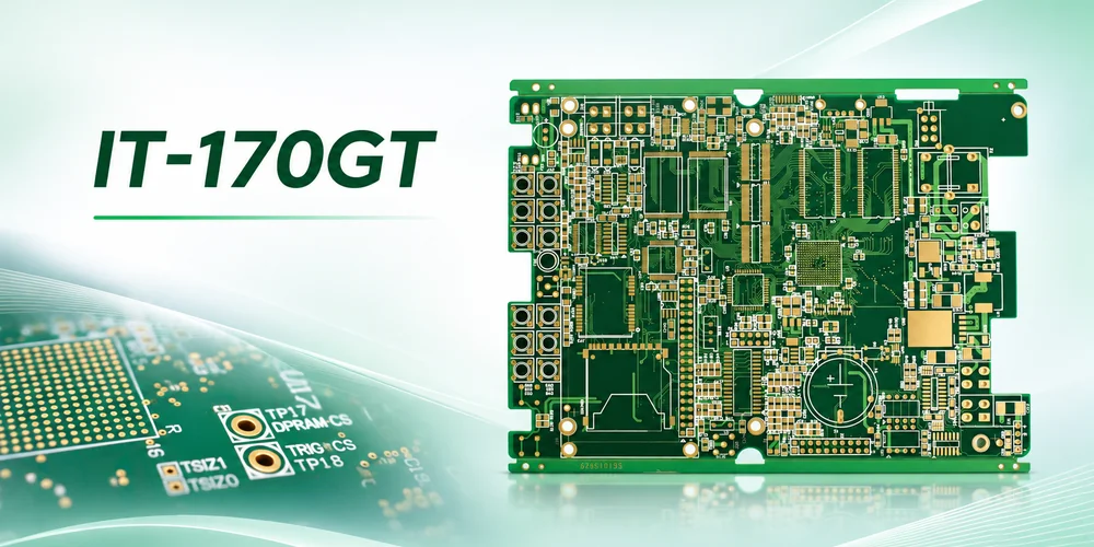
Illustration of a multilayer PCB with plated holes.
ITEQ IT-170GT is a halogen-free, high-Tg laminate and prepreg system for rigid multilayer PCBs. The current datasheet lists a 185°C glass transition temperature by DSC and a 150°C maximum operating temperature for laminate thickness of at least 0.63 mm. For a thick board with plated connector holes, the material is one part of the reliability decision. The drill geometry, inner-layer bond and copper barrel still have to survive the assembly and service conditions.
Read the thermal numbers as separate design inputs
Thermal qualification has three different questions: how the material expands as it heats, what rating applies to the specified construction, and how the fabricated and populated board behaves through its actual temperature history. Those questions require different evidence.
| Ma'lumotlar varag'i elementi | Xabar qilingan natija | uni qanday foydalanish |
|---|---|---|
| Tg (DSC) | 185 ° C | Identifies the glass transition by the stated method. It is not the continuous use rating. |
| Maksimal ish harorati | 150°C at laminate thickness ≥0.63 mm | Read the UL 746 entry with its thickness condition. Do not infer it from overall board thickness or extend it to a populated product. |
| 50–260°C Z-axis expansion | 2.2% at 58% resin content; 1.7% at 48% | Compares expansion of the tested laminate constructions over the stated interval. |
| Td and delamination time | Td 380°C at 5% mass loss; T260 and T288 each >60 min | Distinct laboratory tests. These are not reflow limits or cycle counts. |
| Dk and Df at 10 GHz | 3.9 va 0.0095 | 55% resin content, IPC-TM-650 2.5.5.13; a separate specimen basis from the expansion entries. |
Manba: ITEQ IT-170GT datasheet, Rev. 1.0-26. The CCL row identifies IT-170GT; the prepreg row lists IT-170GTB. Verify construction codes and the applicable safety recognition when releasing the purchase specification.
What does the difference in resin content change?
The 58% specimen shows 0.5 percentage points more through-thickness expansion than the 48% specimen over the published interval. A multilayer board can combine several core and prepreg constructions, with copper patterns that constrain movement. The difference signals that stack composition matters; it does not give the local strain in a plated hole. Specify individual dielectric builds, copper weights and required resin fill. Do not simply select a lower resin content to reduce expansion if it leaves too little resin to fill the etched relief.
Design the connector hole for both fabrication and fit
In a thick multilayer board, the resin and reinforcement expand through the thickness during heating while the bonded copper barrel is constrained. The resulting stress can accumulate through repeated excursions. A thin section of copper, a drill defect or a poor connection to an internal land can become the local weakness. The inspection must therefore represent the hole family most at risk, which may be a smaller plated hole on the same panel rather than the main connector hole.
Hypothetical connector review. A 2.40 mm board calls for a 0.30 mm finished plated hole. If the proposed production drill diameter is 0.38 mm, the nominal board-thickness-to-drill ratio is about 6.3:1. Dividing by the finished diameter gives 8.0:1, a different quantity. The drill value helps review plating access; the finished-hole tolerance governs pin fit and functional acceptance. The calculation does not establish an allowable ratio or prescribe the drill allowance.
Give the fabricator the connector manufacturer’s finished-hole tolerance and annular-ring requirements along with the plated-hole table. In a mechanical drilling review, check registration to buried lands, tool wear and hole-wall quality. Drilling can smear softened resin over inner-layer copper; desmear and conditioning must expose the lands before metallization without creating unacceptable damage. The cross-section should sample copper continuity and minimum thickness through the barrel, including the middle of deep holes, plus the connection to representative internal lands.
For a press-fit connector, coordinate the finished hole, plating and insertion specification with the actual compliant pin. For a soldered connector, the joint must wet and fill according to the assembly requirement; a thick plane connected to the barrel can draw heat away. A change between press-fit and soldered pins can therefore change the fabrication drawing, coupon selection and assembly tooling.
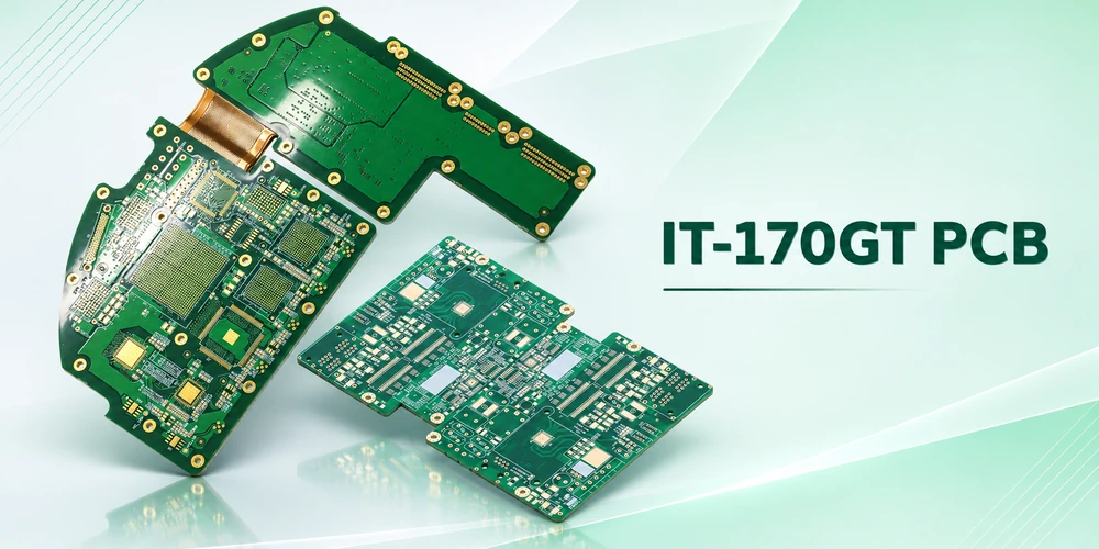
Multilayer PCB illustration. Qualification should represent the actual plated-hole construction.
Diagnose opens that appear only after heat
When an open appears after thermal exposure, first localize the failing net and check when the resistance changes. A continuity test after cooldown can miss an intermittent open. If the application calls for thermal qualification, define a coupon with the relevant hole types, the conditioning and exposure sequence, and when resistance will be measured. Use the applicable IPC-TM-650 methods and purchasing criteria agreed for the build. Typical laminate data do not set board acceptance thresholds.
- Crack through the barrel wall: section the suspect hole at useful orientations and check whether the break passes through plated copper. Review barrel thickness distribution, hole geometry and the thermal history.
- Separation at an inner-layer connection: inspect the specific land-to-barrel interface and look for drilling, smear removal or metallization evidence. Continuous copper on an adjacent barrel wall does not clear the suspect junction.
- Unsound solder joint or poor pin contact: test across the joint or contact separately from the bare-board net. Investigate joint wetting, solder fill or the connector insertion conditions before applying a laminate change as a corrective action.
Preserve the failed unit and compare it with an unstressed specimen when practical. A section through a healthy plane of the same hole can miss a localized crack. Resistance monitoring, physical sectioning and inspection of the assembly answer different parts of the diagnosis.
PCB YASHASH VA YIG'ISH
Planning an IT-170GT PCB build?
Highleap taxta konstruktsiyasi va yig'ish talablarini birgalikda ko'rib chiqishi mumkin.
Include finished hole tolerances, board thickness and the thermal exposures expected at assembly and in use.
Define the first article around the actual heat exposures
Separate the assembly exposure from the service duty cycle. Specify proposed reflow and through-hole soldering steps, planned rework exposures where relevant, and the operating and cycling conditions imposed by the product. Profile areas with different thermal masses on the populated build. A soldered connector near a large plane can heat more slowly than nearby small SMT parts, so a process adjustment must be checked at both locations.
Highleap Electronics reviews these requirements as part of the combined PCB fabrication and assembly scope. Include the controlled stack-up, drill and finished-hole requirements, connector drawings, qualification coupon, BOM and exposure plan in the manufacturing inquiry. The first-article plan can then identify which holes to section, when to monitor resistance and which connector checks belong after assembly.

Muallif haqida
Sabrina
Highleap Electronics kompaniyasida PCB muhandisligi bo'yicha mutaxassis
Sabrina PCB sanoatida 18 yildan ortiq tajribaga ega, CAM muhandisligi va PCB fayllarini ko'rib chiqish sohasida katta tajribaga ega. U ishlab chiqarishga yaroqlilik va jarayonlarning ishonchliligiga e'tibor qaratgan holda, prototipdan tortib hajmli ishlab chiqarishgacha bo'lgan PCB loyihalarini qo'llab-quvvatlaydi.
Uning ishi muhandislik guruhlariga ishlab chiqarish xavfini kamaytirishga va barqaror, yuqori sifatli PCB ishlab chiqarish natijalariga erishishga yordam beradi.

Tavsiya Xabarlar
FPGA mexanik klaviatura PCB ishlab chiqarish va yig'ish
1-rasm. Yig'ilgan Clavier mos yozuvlar klaviaturasi. Bu...
Og'ir mis quvvatini boshqarish uchun IT-858G avtomobil PCBlari
IT-858G PCB avtomobil elektronikasi va... da qo'llaniladi.
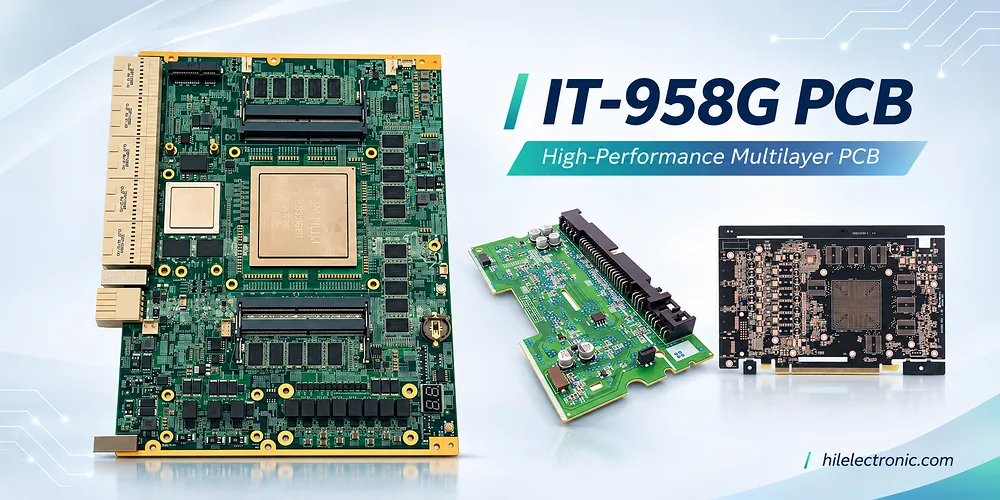
Yuqori tezlikdagi serverlar va orqa panellar uchun IT-958G PCB
Server va yuqori tezlikdagi kompyuterlar uchun IT-958G ko'p qatlamli PCB namunalari...
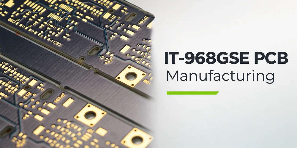
Yuqori tezlikdagi tarmoq uchun IT-968GSE PCB
Ultra past yo'qotishli kalit va... uchun IT-968GSE PCB illyustratsiyasi
PCB uchun narxni qanday olish mumkin
Keling, siz uchun DFM/DFA tahlilini oʻtkazamiz va sizga hisobot bilan qaytamiz. Veb-saytimiz orqali fayllaringizni xavfsiz yuklashingiz mumkin. Sizga narx taklif qilish uchun bizga quyidagi ma'lumotlar kerak bo'ladi:
-
- Gerber, ODB++ yoki .pcb, spetsifikatsiya.
- Agar yig'ishni talab qilsangiz, BOM ro'yxati
- miqdor
- Vaqtni aylantirish
PCB ishlab chiqarishga qo'shimcha ravishda, biz PCB dizayni, PCBA va kalit echimlarni o'z ichiga olgan keng qamrovli elektron xizmatlarni taklif etamiz. Prototip yaratish, dizaynni tekshirish, komponentlarni qidirish yoki ommaviy ishlab chiqarish bo'yicha yordam kerak bo'ladimi, biz loyihangiz muvaffaqiyatini ta'minlash uchun oxirigacha yordam beramiz.
PCBA xizmatlari uchun BOM (Materiallar ro'yxati) va har qanday maxsus montaj ko'rsatmalarini taqdim eting. Shuningdek, biz dizaynlaringizni ishlab chiqarish va yig'ish uchun optimallashtirish uchun DFM/DFA tahlilini taklif qilamiz, bu esa silliq ishlab chiqarish jarayonini ta'minlaydi.