
Lehim niqobi ko'prigi nimani anglatadi va uni qanday oldini olish mumkin?

Lehim niqobi ko'prigi nima?
A solder mask bridge, also called a solder mask dam or web, is the narrow strip of insulating solder mask between adjacent pad openings. It is normally an intentional feature that helps keep solder on separate pads during assembly. A solder bridge is different: it is an unwanted conductive connection made by solder between conductors that should remain separate.
The solder mask pattern leaves designated pads and other required copper areas exposed. Where the spacing and fabrication process permit, mask remains between neighboring openings. The finished dam width depends on pad geometry, mask expansion, registration tolerance and the fabricator’s process capability. A PCB soldermask specification should identify openings, registration and material requirements rather than only a color.
An intact solder mask dam is insulating and does not short adjacent pads. Problems arise when a dam is too narrow to manufacture reliably, is missing or damaged, or when misregistered mask covers a surface that must be soldered. A missing dam can increase solder-bridging risk, but assembly controls also matter.
Review pad spacing, solder mask openings and minimum finished dam width with the fabricator before release. Inspection should distinguish missing or misplaced mask from actual excess solder; the two defects require different corrective actions.
Sizning PCB lehim bilan niqoblash jarayoniga qanday ta'sir qiladi

Lehim bilan niqoblash jarayoni bosilgan elektron platalarni (PCB) ishlab chiqarish va ishlashda hal qiluvchi rol o'ynaydi. Lehim bilan niqoblash jarayoni PCBga qanday ta'sir qiladi:
- Helps Prevent Solder Bridges: A retained mask dam separates adjacent exposed pads and discourages solder from spreading between them. It supports assembly yield but cannot compensate for excessive paste, poor placement or an unsuitable soldering process.
- Works with the Stencil Design: Paste volume is governed primarily by stencil aperture geometry, stencil thickness and printing conditions. Solder mask does not directly reduce the quantity of paste required for a sound joint.
- Protects Covered Copper: Properly applied and cured solder mask helps protect copper against handling damage, oxidation and contamination. It is not a hermetic seal or a substitute for product-specific environmental protection.
- Supports the Insulation System: Electrical insulation depends on the complete board construction and applicable qualification. Do not assume a mask coating establishes a particular voltage rating, prevents corona, or allows required creepage and clearance distances to be reduced.
- Does Not Eliminate Tin Whiskers: Solder mask is not a general remedy for tin-whisker growth on component finishes. Finish selection and any coating-based mitigation require a separate reliability assessment; even conformal coatings have limitations.
Solder mask protects covered copper and helps maintain separation between solderable areas. Its practical benefits depend on accurate artwork, registration, adhesion and cure. Agree the mask requirements and inspection criteria with the fabricator, and assess insulation or environmental performance against the finished product requirements.
Solder Bridging and Other Assembly Defects
A solder bridge can short neighboring conductors. The following assembly defects are separate failure modes and should not all be attributed to solder bridging:
Suvsizlanish va namlantirmaslik: Dewetting occurs when solder retreats after initially wetting a surface; non-wetting occurs when a sound wetted interface does not form. Surface condition, oxidation, contamination, flux activity and the thermal profile should be investigated.
Pinholes and Blowholes: Gas escaping while a solder joint solidifies can leave small or larger openings. Investigate moisture, contamination, flux behavior and plated-through-hole quality according to the joint and process involved.
Ko'tarilgan prokladkalar: Excessive heating, prolonged rework or mechanical force can separate a pad from the laminate. Avoid pulling on a component or braid before the solder has fully melted, and assess any damaged pad before repair.
Qabr toshlarini qo'yish: A small chip component can stand on one end during reflow when wetting forces at its two terminations become unbalanced. Pad geometry, thermal balance, paste deposits, placement and termination solderability are relevant causes; it is not the same defect as a solder bridge.
Haddan tashqari lehim: Too much paste, unsuitable stencil apertures, placement errors or an unsuitable wave/selective-soldering process can leave unwanted solder connections. Diagnose the process actually used rather than applying one conveyor-speed rule to every assembly.
These issues can affect the functionality, reliability, and performance of the soldered connections on the PCB. To mitigate these problems, it is important to follow proper soldering techniques, ensure adequate plating and cleanliness of the board, and use components that are compatible with the soldering process. Additionally, inspection and quality control measures should be implemented to detect and address any soldering defects before the PCB is used in electronic devices.
How to Preserve Solder Mask Dams and Reduce Solder Bridges
To reduce unwanted solder bridges in your PCB yig'ilishi, you can follow a set of precautions and best practices throughout the design, manufacturing, and assembly processes. The following checks address the mask pattern and the assembly process:
- PCB dizaynini tekshiring: Carefully review your PCB design to ensure that it meets the best practices for manufacturability, especially for surface mount and through-hole components. Use the applicable IPC design requirements and the fabricator’s documented capabilities for the actual board construction.

- Set Mask Openings from the Fabrication Rules: Define mask expansion and registration allowances with the fabricator and component footprint requirements. There is no single relief range that suits every SMT pad pitch or mask process.
- Validate the Reflow Profile: Use the solder paste supplier’s process window and component temperature limits. Measure the board profile before changing it; simply extending time above liquidus can damage the assembly or create other defects.
- Retain Manufacturable Mask Dams: Use dams between pads where the finished width and registration can be maintained. Confirm the minimum capability for the selected mask, copper and process rather than applying a universal 0.004-inch rule.
- Teshik qismlari uchun qo'rg'oshin uzunligini ko'rib chiqing: Teshikdan o'tuvchi komponentlar uchun mos keladigan uzunlikni hisobga oling. Taxta qalinligi, komponent o'lchami va lehim usuli kabi omillar kerakli qo'rg'oshin uzunligiga ta'sir qilishi mumkin. Ko'prikning oldini olish uchun to'g'ri uzunlikni aniqlash uchun PCB ishlab chiqaruvchisi bilan maslahatlashing.
- Control Solder Paste Volume: Review stencil apertures, thickness and printing consistency when excess paste contributes to bridging. Reduce deposits only within the requirements for reliable solder joints.
- Choose Pad Definition Deliberately: Solder-mask-defined and non-solder-mask-defined pads have different geometry and reliability implications. Follow the component manufacturer’s footprint guidance; do not convert pads to mask-defined solely because a dam is difficult to manufacture.
- Review Pad and Hole Geometry: Check component pitch, pad spacing, drill sizes, annular rings and mask openings together. Geometry should satisfy both electrical connectivity and fabrication/assembly requirements.
- Apply and Inspect the Mask: Check that required solderable pads and test points remain exposed, and that mask coverage, registration, adhesion and cure meet the agreed specification.
- Use Suitable Fiducials: Correctly placed and unobstructed fiducials support consistent placement alignment. They address placement accuracy rather than creating or repairing solder mask dams.
- Coordinate Fabrication and Assembly: Resolve narrow mask webs, grouped openings and fine-pitch soldering risks with both teams before release. Record approved artwork changes instead of making undocumented pad or mask modifications.
A reliable result combines a manufacturable mask pattern with controlled paste printing, placement and soldering. Inspect the bare board and assembled joints separately so the root cause of a defect can be identified.
How to Repair an Unwanted Solder Bridge
The steps below apply to excess conductive solder, not to an intact solder mask dam. Disconnect power and safely discharge stored energy before rework. Missing or damaged mask requires a separate approved mask-repair process.
Kerakli asboblar va materiallar:
- Nozik uchi va sozlanishi haroratni nazorat qiluvchi lehimli temir
- Lehim tayoqchasi (ochish uchun ortiqcha oro bermay)
- Lehim oqimi
- Multimetr (ixtiyoriy, sinov uchun)
- Nam shimgichni yoki nam mato (lehimli temir uchini tozalash uchun)
Ish tartibi:
- Prepare Your Soldering Iron: Select a suitable tip and temperature-controlled station. Use a rework setting appropriate to the solder alloy, joint thermal mass, braid and component limits; a universal 150–250°C setting is not an adequate process instruction.
- Monitor Heat Input: Use adequate tip contact and heat transfer while limiting dwell time. If solder does not flow, reassess the tool, flux and thermal mass rather than repeatedly increasing temperature or holding the iron against the pad.
- Remove Excess Solder Carefully: For accessible joints, compatible flux and a suitable iron tip can help draw away excess solder. Keep separate joints distinct and avoid scraping or pulling on pads. Use braid when controlled removal with the tip alone is insufficient.
- Lehim tayoqchasidan foydalaning: Agar sirt tarangligining o'zi ko'prikni olib tashlamasa, siz lehim tayoqchasidan foydalanishni davom ettirishingiz mumkin. Buni qanday qilish kerak:
- Apply compatible flux to the solder bridge if required by the chosen braid and rework process.
- Lehim tayoqchasini to'g'ridan-to'g'ri ko'prik ustiga qo'ying, u butun ko'prikli maydonni qamrab olishiga ishonch hosil qiling.
- Lehimlash temirining uchini tayoq ustiga qo'ying, issiqlikni uzatish uchun yumshoq bosim o'tkazing.
- When the solder melts, allow the braid to absorb it. Lift the iron and braid away together while the solder is still molten; do not pull on braid that has solidified onto a pad.
- Tiqilgan tayoqni almashtiring (agar kerak bo'lsa): Agar lehim tayoqchasi so'rilgan lehim bilan tiqilib qolsa, jarayonni samarali davom ettirish uchun uni yangi qism bilan almashtiring.
- Lehimlash temirining uchini tozalang: vaqti-vaqti bilan lehim dazmolining uchini nam shimgichni yoki nam matoga artib tozalang. Toza uchi ta'mirlash vaqtida yaxshi issiqlik uzatishni ta'minlaydi.
- Inspect the Repair: After cooling and appropriate cleaning, inspect the joints under magnification for bridges, disturbed joints, lifted pads and mask damage. With power off, use the schematic and suitable electrical tests to check the affected nets; a continuity beep alone cannot distinguish an intended low-resistance path from a short.
- Lehimni qayta qo'llang (agar kerak bo'lsa): Agar ko'prikni olib tashlash lehim birikmasini olib tashlashga olib keladigan bo'lsa, komponentlar orasidagi toza va mustahkam lehim aloqasini tiklash uchun qo'shimcha lehimni qo'llang.
Keep rework within the assembly’s permitted thermal exposure and repair requirements. Escalate inaccessible joints, damaged pads or uncertain electrical results to a qualified technician rather than continuing to heat the board.
xulosa
A solder mask bridge is normally a useful insulating dam between pad openings. A conductive solder bridge is an assembly defect. Keeping these terms distinct makes design reviews, inspection and repair more effective: preserve manufacturable mask dams, control solder deposition and reflow, and repair only the actual defect identified.

Haqida Maqolalar
Yuqori sifatli qattiq PCB elektron platalarini ishlab chiqarish xizmatlari
Qattiq PCBlar FR4 PCB ning an'anaviy turi bo'lib, odatda shisha tolali materiallardan tayyorlangan qattiq substratni o'z ichiga oladi.
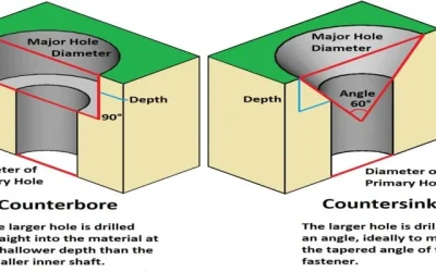
PCB o'rnatish teshiklari: Counterbore va Countersinkni tushunish
Qarama-qarshi va qarama-qarshi teshiklar o'rtasidagi tanlov turli omillarga, shu jumladan vint turiga va dastur talablariga bog'liq.
Umumiy PCB burg'ulash jarayonidagi nosozliklar va echimlar
Ushbu maqolada PCB burg'ulash jarayonining keng tarqalgan nosozliklari, ularning sabablari va burg'ulash jarayonini silliq va samarali ta'minlash uchun echimlar muhokama qilinadi.