
IT-968GSE PCB for High-Speed Networking
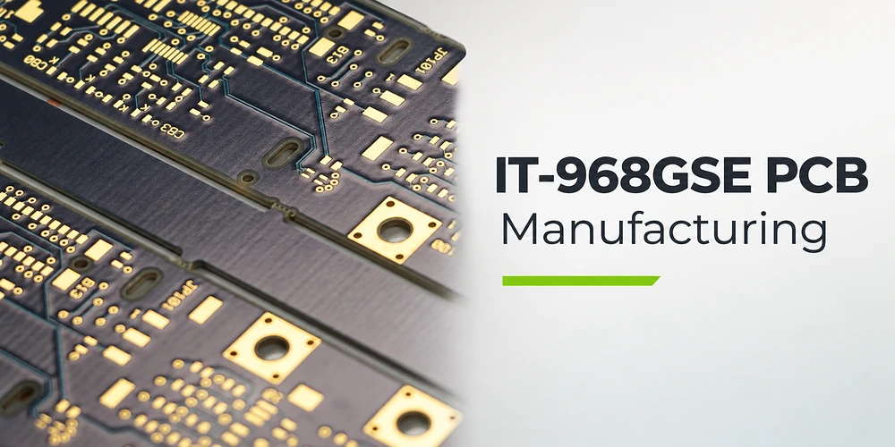
IT-968GSE PCB illustration for ultra-low-loss switch and telecom board planning.
400G-class switch cards and high-speed telecom boards can be sensitive to small differences in dielectric constant, copper roughness and via transitions. IT-968GSE is an ultra-low-loss ITEQ laminate and prepreg option, but its published Dk/Df values depend on the resin-content basis of the test specimen. Highleap’s fabrication and assembly review for an IT-968GSE board therefore starts with the specified resin basis, pressed dielectric thickness, foil profile, differential-pair geometry and connector launches—not a generic material label.
ITEQ reports 10 GHz Dk/Df of 3.16/0.0036 for a 55%-resin specimen and 2.84/0.0029 for a 70%-resin specimen. These are not interchangeable values for the same pressed layer. A 100G/400G-class channel also requires control of copper texture, etching, return paths, vias and connector launches, not simply a low Df grade name.
IT-968GSE Dk and Df: Why Resin Content Cannot Be Ignored
The manufacturer publishes two dielectric sample bases for IT-968GSE. At 10 GHz, the 55%-resin specimen is listed at Dk 3.16, Df 0.0036, while the 70%-resin specimen is Dk 2.84, Df 0.0029. Neither pair is a universal value for every finished board. Differences in reinforcement, resin fraction, frequency, foil profile and test setup can make a manufactured transmission line respond differently.
| ITEQ IT-968GSE property | 55% resin specimen | 70% resin specimen |
|---|---|---|
| Dk při 1 GHz | 3.33 | 3.00 |
| Dk při 5 GHz | 3.17 | 2.87 |
| Dk při 10 GHz | 3.16 | 2.84 |
| Df při 1 GHz | 0.0028 | 0.0022 |
| Df při 5 GHz | 0.0032 | 0.0024 |
| Df při 10 GHz | 0.0036 | 0.0029 |
Other supplier-published values include Tg of 175°C by TMA, decomposition temperature of 400°C at 5% weight loss and Z-axis expansion of 2.3% from 50°C to 260°C. They provide context for high-temperature handling and via reliability, but a completed PCB still requires its own acceptance plan.
Why a 0.32 Dk difference matters
For a simplified homogeneous transmission medium, propagation delay varies approximately with the square root of effective permittivity. Using the two illustrative material values above gives a square-root ratio of √(3.16/2.84) ≈ 1.055, or roughly a 5.5% difference in propagation-delay factor. This is not a measured IT-968GSE board delay and does not mean every microstrip changes by 5.5%; actual fields also occupy air and other dielectrics. The calculation shows why material-property selection cannot be disconnected from a real stack-up.
For production, resin-fraction data used to calculate the pressed dielectric must be treated as a construction variable rather than a decorative datasheet column. Core and prepreg selection, dielectric thickness and copper pattern collectively determine the final geometry seen by the signal.
IT-968GSE PCB manufacturer requirements for 400G switch cards
For a detailed engineering quote on a 400G switch PCB, the laminate and prepreg form, pressed stack-up, copper-foil treatment, differential impedance, operating frequency range and channel-loss criteria need to be defined. The system label “400G” alone is not enough: lane signaling, route length, connector transitions and permitted insertion loss determine the actual electrical requirements. These details can be developed after the first discussion; an initial inquiry can begin with the board type and approximate quantity.
Highleap can review the PCB and PCBA documentation for IT-968GSE projects, including whether the specified material construction and foil are sourceable and whether the requested geometry and test scope are feasible. High-speed laminate selection and assembly of high-speed connectors or packages should be treated as linked manufacturing decisions.
400G Switch PCB Stack-Up Design with IT-968GSE
Design equations are only as good as the dielectric construction
A field solver needs a dielectric model consistent with the actual routing layer. A 70%-resin prepreg sample and a 55%-resin laminate sample may both be legitimate supplier data, but they cannot be substituted blindly as inputs for one trace. The right model may need anisotropy, frequency dependence and a construction-specific effective permittivity. Those effects become more visible in long routes, high-density differential pairs and regions where the trace width is comparable to the reinforcement pattern.
A tightly coupled pair is not a guarantee of balanced timing. Unequal exposure to glass bundles, asymmetric reference shapes and unequal via launches all contribute differential skew or common-mode conversion. Layout and materials engineering must therefore be coordinated before selecting one nominal Dk for the whole design.
In high-speed digital systems, a low-Df substrate is not enough to deliver an acceptable channel. The signal travels through traces, transitions and interfaces whose fields depend on plane structure and local geometry. Differential routing and return-path design for high-speed links must be reconciled with the approved reference planes, conductor cross-section, pressed dielectric thickness and copper-foil treatment on each critical layer.
A stack-up model should be construction-specific:
- Pro páskové vedení, the fields are largely inside the board dielectric, so sample-dependent Dk matters strongly to impedance and delay.
- Pro mikropáskový, part of the field is in air, and solder mask, adjacent copper and geometry alter the effective properties.
- Pro diferenciální páry, trace separation and asymmetry affect both impedance and mode conversion; they cannot be corrected merely by replacing one Dk number.
- Pro via transitions, reference-plane changes, antipad geometry, stubs and launch structures can dominate localized reflections.
The nominal material data should feed a field solver alongside the actual layer build. Finished-line impedance targets and the production coupon method turn the model into a measurable fabrication requirement: target, tolerance, test structure and approved measurement method must all be defined. A board labeled “IT-968GSE, 100 ohms” is missing information required for repeatable manufacturing.
The PCB glass-weave effect may be relevant where closely coupled traces have a long parallel route over nonuniform reinforcement. Effective-Dk differences can generate pair skew even while average impedance remains acceptable. Available mitigation depends on route geometry, selected reinforcement and the performance margin of the link.
Differential-pair skew and glass-weave effects in low-loss PCBs
The effective dielectric surrounding each trace of a tightly coupled differential pair may differ where glass bundles and resin-rich regions lie along the route. That can contribute to local skew even when the nominal Dk is correctly chosen. Differential-pair orientation, routing length, spread-glass or other approved glass styles, and the resulting fabrication constraints should be reviewed together.
The solution is not to assume that every IT-968GSE sheet has the same glass distribution. The approved glass style and resin percentage belong in the stack-up or material specification when they materially affect the electrical model.
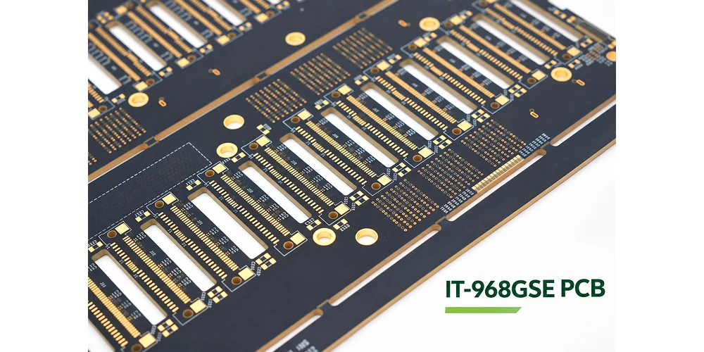
Dense interconnect geometry for reviewing IT-968GSE routing, copper profile and fabrication requirements.
Ultra-Low-Loss Multilayer PCB Manufacturing: Foil and Etching
At elevated frequencies, current crowds toward the copper surface. Surface roughness, conductor shape, finished width and return-path geometry therefore contribute to insertion loss. A material with an excellent supplier Df can still produce an unexpectedly lossy line if the foil treatment or trace geometry differs from the simulation assumption.
Volba low-profile copper foil options for conductor-loss control should be tied to both electrical modeling and mechanical process needs. Smoother foil may reduce conductor loss, but copper-to-resin adhesion and the required manufacturing route must also be considered. Different foil families are not interchangeable simply because their nominal thickness is the same.
| Physical detail | Elektrické následky | Řízení výroby |
|---|---|---|
| Foil surface profile | Conductor attenuation changes with frequency | Approve foil grade and treatment with the stack-up |
| Etched trace trapezoid | Actual line impedance differs from CAD width | Model and measure finished trace geometry |
| Local plating variation | Surface cross-section and width can change | Process control and cross-section evidence where specified |
| Resin/glass distribution | Local effective Dk can shift delay and skew | Approved prepreg/core schedule and layout review |
| Reference-plane clearance | Return path can detour near vias or cutouts | Via and plane-transition modeling |
Interakce mezi foil treatment and surface finish in GHz signal paths illustrates why copper specification belongs in the RFQ. Substituting a different foil treatment can change channel behavior even when the resin family is unchanged.
VÝROBA A MONTÁŽ DESEK PLOŠNÝCH PLOŠIN
Developing a high-speed switch board around IT-968GSE?
Highleap can discuss the switch-card application, target data rate and the related PCB fabrication and assembly requirements.
První dotaz je jednoduchý. No complete stack-up or channel-test package is needed to start. A short description of the switch-card application and target data rate is enough; pressed-dielectric and copper-foil details can be reviewed later.
IT-968GSE Fabrication Risks: Registration, Plating and Channel Verification
The test coupon should reproduce the loss-producing structure
A short, straight microstrip impedance coupon may confirm line impedance but miss the insertion-loss penalties of the production stripline, treated foil, long route or backdrilled via transition. Where S-parameter evidence is required, the coupon or test vehicle should represent the critical signal layer, conductor profile and expected reference planes. Probe launches and fixture loss need to be accounted for in the measurement plan; otherwise the reported loss includes the test setup and cannot be compared fairly with the channel model.
Time-domain reflectometry can help locate impedance steps, while frequency-domain methods can quantify return and insertion loss across the agreed band. The measurement method, calibration/de-embedding approach, target frequency and pass/fail limits should be documented before a qualification lot is launched. A bare-board electrical continuity test does not supply this evidence.
ITEQ positions IT-968GSE for advanced high-speed switch and communications equipment. That application context increases the importance of large multilayer panel registration, long signal routes, dense connector footprints and dimensional consistency across repeated builds. Material selection alone cannot make a high-speed channel tolerant of process drift.
At board level, switch-card architecture and connector density in large Ethernet systems also influence layer assignment, via transitions and the placement of representative electrical coupons.
The fabrication drawing needs to align the actual stack-up, material callout and coupon plan. For complex builds, press-cycle control of dielectric thickness and layer registration must be coordinated with drilling and metallization so plated-hole integrity and signal-transition geometry are preserved. A via can pass continuity while an excessive stub or unintended antipad still creates a reflection.
Verification should separate three outcomes:
- Bare-board construction: cross-section, dielectric thickness, copper geometry, plating and registration satisfy the released drawing.
- Transmission-line impedance: coupons on representative layers meet the specified tolerance under the agreed method.
- Channel performance: where the product requires it, insertion-loss/return-loss measurements or correlation to simulated S-parameters assess the whole routing environment.
A multilayer communication-board layout with dense connector transitions might pass the first two checks and still require connector-launch tuning. Conversely, a poor coupon result may be traced to pressed dielectric thickness rather than the material’s published Dk. Treating these as separate failure hypotheses speeds corrective action.
For via-intensive projects, HDI PCB reliability depends on a representative build-up process and verification of critical interfaces. IT-968GSE’s high-Tg description does not eliminate the risk of microvia interface defects or defects introduced during sequential lamination.
When a 400G PCB manufacturer needs S-parameter coupon testing
For a long or margin-sensitive channel, an impedance coupon alone may not expose losses from rough foil, backdrilled stubs or transitions. An S-parameter coupon that reproduces the critical layer and geometry can support insertion-loss verification, with fixtures and calibration addressed in the test procedure. The required measurement band and limits must come from the design specification.
A supplier quote should state whether it includes bare-board continuity, impedance checks, additional insertion-loss measurements or system-level tests after PCB assembly. These operations answer different questions and should not be presented as interchangeable.
Those requirements should be tied to production controls for high-speed multilayer switch boards, including registration, copper treatment, via transitions and the agreed electrical verification.
IT-968GSE vs IT-968G and IT-988GL: Avoid Automatic Substitution
Do not confuse marketing application classes with guaranteed lane performance
A supplier may position a laminate for 100G/400G switches, but an Ethernet interface label does not reveal a board’s signaling rate per lane, channel length, connector count or equalization capability. Two products in the same switch generation can have dramatically different PCB loss budgets. Material selection must therefore follow the specific channel requirements rather than a generic statement that a material “supports 400G.”
Any substitution should update the stack-up table, signal simulation and qualification scope; where approved copper treatment or glass construction changes, the revised material specification should also be reflected in the purchase documents.
The ITEQ grade suffix matters. The supplier describes IT-968G, IT-968GSE and IT-988GL as distinct material options with different electrical property sets. Even when all are suitable for considering a high-speed stack-up, substituting one for another changes the field-solver inputs, potentially the foil/resin construction and sometimes the production process.
| Kandidát | ITEQ published Dk / Df at 10 GHz | Specimen basis | What the selection changes |
|---|---|---|---|
| IT-968GSE | 2.84 / 0.0029 | 70% resin | Low effective-Dk modeling, ultra-low dielectric loss |
| IT-968G | 3.26 / 0.0039 | 70% resin | Different impedance/loss basis despite similar family naming |
| IT-988GL | 3.21 / 0.0033 | 70% resin | Different laminate expansion and electrical construction |
These are sample values, not measured losses of identically built channels. Any grade change should be evaluated for thickness, conductor geometry, dielectric behavior and electrical qualification before release. A comparison of dielectric values across high-speed laminate families should use matched frequency, resin content and test construction rather than select the lowest printed Df by default.
For PCB assembly, connector seating, BGA soldering, reflow profile and rework procedures should be coordinated with the approved bare-board construction. Highleap Electronics can review an IT-968GSE PCB/PCBA project for material availability, manufacturable stack-up, agreed fabrication tests and assembly scope when supplied with the released design and qualification requirements.

O autorovi
Helen Chongová
Konzultant pro řešení desek plošných spojů a manažer rozvoje zámořského obchodu ve společnosti Highleap Electronics
Helen podporuje mezinárodní inženýrské týmy s komplexními řešeními pro výrobu a montáž desek plošných spojů a pomáhá projektům přejít od rychloobrátkových prototypů ke stabilní hromadné výrobě. Její zkušenosti zahrnují vysokofrekvenční a RF desky, komplexní vícevrstvé struktury, technologie pevných, flexibilních a flexibilních desek plošných spojů v různých odvětvích.
Převodem technických požadavků do praktických výrobních plánů pomáhá zákazníkům zlepšit vyrobitelnost, snížit rizika a optimalizovat náklady a dodací lhůty – a zároveň udržovat konzistentní kvalitu ve velkém měřítku.

doporučené příspěvky
Výroba desek plošných spojů Arlon 35N a laminace polyimidem
Ilustrace výroby desek plošných spojů. Potvrďte zadané...
Výroba desek plošných spojů Arlon 45NK s nízkým CTE v Číně
Ilustrace výroby desek plošných spojů. Potvrďte zadané...
Výroba desek plošných spojů Arlon 85HP v Číně
Ilustrace výroby desek plošných spojů. Potvrďte zadané...
Výroba desek plošných spojů Arlon 86HP HDI
Ilustrace výroby desek plošných spojů. Potvrďte zadané...
Jak získat cenovou nabídku na desky plošných spojů
Provedeme pro vás analýzu DFM/DFA a ozveme se vám se zprávou. Své soubory můžete bezpečně nahrát prostřednictvím našich webových stránek. Pro vypracování cenové nabídky potřebujeme následující informace:
-
- Gerber, ODB++ nebo .pcb, spec.
- Seznam kusovníků, pokud požadujete montáž
- Množství
- Čas otáčení
Kromě výroby desek plošných spojů nabízíme komplexní škálu elektronických služeb, včetně návrhu desek plošných spojů, výroby desek plošných spojů a komplexních řešení. Ať už potřebujete pomoc s prototypováním, ověřováním návrhu, zajištěním zdrojů součástek nebo hromadnou výrobou, poskytujeme komplexní podporu, abychom zajistili úspěch vašeho projektu.
Pro služby PCBA prosím poskytněte kusovník (BOM) a případné konkrétní montážní pokyny. Nabízíme také analýzy DFM/DFA pro optimalizaci vašich návrhů z hlediska vyrobitelnosti a montáže a zajištění plynulého výrobního procesu.