
Highleap Electronics / PCB + PCBA Manufacturing
Speciální desky plošných spojů pro OEM produkty
Compare board constructions, special features and assembly options before preparing your manufacturing files.
- Výroba zakázkových desek plošných spojů
- Special PCB structures
- SMT / THT / turnkey PCBA
Vyžádejte si cenovou nabídku na desky plošných spojů
Tell us what you need, including your board type, quantity and target delivery date.
Highleap Electronics manufactures custom circuit boards and assembled PCBAs for OEM and ODM products. Our manufacturing scope covers standard FR-4, multilayer, flexible and rigid-flex boards, keyboard circuit boards, LED circuit boards, power supply boards, ceramic circuit boards, thick copper circuit boards, RF and high-frequency designs, HDI structures and special-process constructions. Customers can source bare PCBs or coordinate fabrication, approved component procurement, SMT and through-hole assembly, programming, inspection and agreed functional testing through one project.
Product applications include mechanical keyboards, industrial keypads, LED lighting and displays, AC/DC power supplies, solar inverters, EV charging equipment, battery systems, PLC controllers, network equipment, medical instruments, automotive electronics and IoT devices. These products may also require gold fingers, plated half-holes, cavities, controlled-depth routing, filled vias, embedded copper inserts or selective surface finishes. Highleap reviews the product requirements and special fabrication features together so that the bare-board design remains compatible with assembly and inspection.
Highleap offers standard multilayer, flexible, rigid-flex, high-frequency, heavy copper, metal-core and ceramic circuit board solutions described on our PCB fabrication service page. For unusual or combined structures, materials, production routes, available inspection methods and lead time are confirmed during engineering review. This page outlines the product families and special circuit board configurations that can be discussed for build-to-print manufacture and assembly.
Custom Circuit Board Manufacturing and Assembly
We supply customer-defined circuit board fabrication and assembly, rather than restricting projects to a fixed catalog of board sizes or one consumer product category. A single hardware system may use a high-current power PCB, a fine-pitch processor PCB, a flexible cable-replacement circuit and a front-panel keypad circuit board. Those assemblies can be identified, quoted and released as related parts with controlled revisions.
Single-Sided, Double-Sided and Multilayer Circuit Boards
Highleap fabricates single-sided circuit boards, double-sided circuit boards and multilayer circuit boards for custom electronics and equipment assemblies. Standard rigid FR-4 options support control circuits, keyboards, sensor nodes and power-interface boards; custom multilayer construction supports more power and ground layers, dense BGA routing, impedance control and complex component combinations.
A 2-layer keyboard PCB may require precisely located switch footprints and USB connections, while a 6-layer controller board may combine MCU logic, isolated communications and a power section. An 8- or 12-layer communication board often needs controlled dielectric spacing, reference planes and defined via structures. For fine-line or ultra-high-layer-count projects, the approved stack-up and fabrication tolerances determine feasibility—not a general statement that every layer count can be produced.
Fine-line, ultra-thin and thick multilayer circuit boards
Highleap can assess fine-line and multilayer circuit board designs for processors, industrial backplanes, communication equipment and compact electronic modules. Trace geometry, BGA pitch, via registration, board thickness and dielectric control are separate engineering constraints that must be stated on the fabrication drawing.
The terms below describe finished-board constraints and construction choices, not an assurance that any requested dimension is achievable without DFM.
Fine-line, board-thickness and stack-up configurations
For high-speed backplanes, controlled impedance and via-stub removal may matter more than a headline layer count. For ultra-thin or very thick boards, panel handling and assembly tooling also need review. A stack-up may combine several of these requirements, but quotation should identify each separately.
Programs involving a high-frequency or high-speed PCB construction can specify copper profile, low-loss materials and test coupons when the electrical design requires them. A material specification does not by itself guarantee link-level performance.
For an assembled multilayer circuit board, send the approved fabrication data with the BOM and component placements. Surface finish, solder-mask clearances, panel support and electrical-test coupon requirements must remain compatible with the selected SMT or through-hole route.
Keyboard, Keypad and Human-Machine Interface Circuit Boards
Highleap manufactures custom keyboard circuit boards for mechanical keyboards, gaming keyboards, ergonomic keyboards and industrial keypads, with optional SMT/THT assembly, controller programming and project-defined key testing. Náš keyboard PCB manufacturing and assembly service covers OEM-specified board outlines, switch arrays, connector footprints and component population.
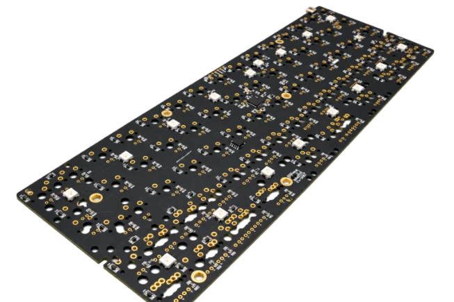
Mechanical keyboard, hot-swap keyboard and RGB keyboard circuit boards
We can assess a mechanical keyboard circuit board with through-hole switch contacts, a hot-swap keyboard PCB with specified socket footprints, or a gaming keyboard circuit board combining per-key RGB LED assembly, anti-ghosting diode matrices and USB-C connectivity. Compact 60%, 65%, 75%, TKL and full-size keyboard PCBs require different key spacing, plate mounting, stabilizer clearances and flex or split-board interconnections. The key matrix and fitted/DNP variants should be unambiguous in the BOM and assembly drawings.
Pro split ergonomic keyboard circuit boards a wireless keyboard PCBA, the manufacturing package can include daughterboards, battery or charging sections, RF modules and inter-board connectors. Firmware flashing and matrix verification can be added when the customer provides compatible files and test instructions. Hall-effect keyboard designs or other specialist switch technologies need a separate review of sensors, magnet locations, mechanical tolerances and calibration method.
Membrane keypad, carbon ink keypad and touch control circuit boards
Equipment interfaces may instead use membrane keypad circuit boards, carbon ink keypad circuit boards, capacitive touch circuit boards, HMI controller boards or compact front-panel indicator PCBAs. Carbon ink contact resistance, key-pad surface geometry, electrode finish and protective overlay are specified according to the approved switch technology. The same program may require an LCD/display board, indicator LED board and separate keyboard controller. Highleap can quote them as a matched assembly set rather than a bare PCB alone.
For prototype approval, the useful evidence is correct component placement, switch-matrix scanning, debounce or firmware configuration, RGB LED channel operation and connector/mounting fit as required. The final keycap, housing or water-ingress performance is a separate end-product qualification unless included in the agreed box-build scope.
LED Lighting, Display and Backlight Circuit Boards
Highleap supplies LED circuit board fabrication and assembly for high-power lighting, displays, indicator products and LED driver electronics. Typical requests include aluminum LED circuit boards, metal-core LED PCBs, LED driver circuit boards, RGB LED controller boards, high-power LED array boards, LED matrix circuit boards and flexible LED strip circuit boards.
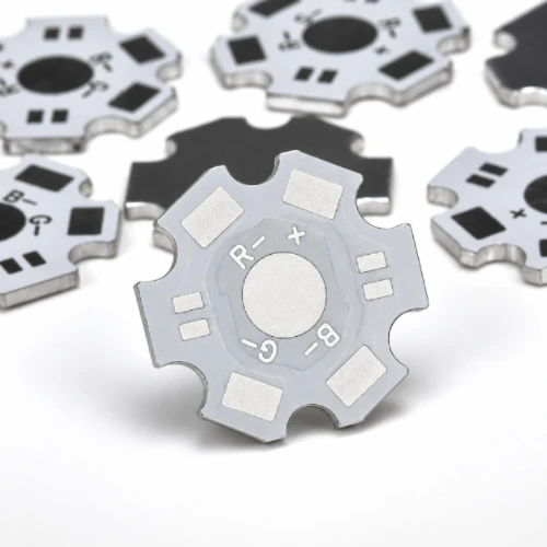
Aluminum LED circuit boards, high-power LED boards and lighting modules
Vysoce výkonný LED light engine PCB may use an aluminum metal-core substrate or a copper-base circuit board with a defined dielectric and heatsink interface. LED street-light boards, automotive lamp boards, industrial high-bay LED modules, UV LED boards and horticultural lighting PCBs may require different substrate, LED package, thermal pad and mechanical mounting options. Highleap can evaluate metal-core circuit board fabrication for those specified builds.
For LED assembly, the customer should supply the approved LED manufacturer and orderable part number, binning rules, polarity, placement orientation, thermal-interface requirements and any color/brightness consistency criteria. An aluminum PCB improves one part of the thermal path, but it does not independently establish the module’s lumen output, junction temperature, lifetime or luminaire certification.
LED driver PCB, LED display board and LCD backlight circuit board
Highleap can also coordinate LED power supply circuit boards, dimmable LED driver PCB assemblies, addressable RGB controller boards, digital signage circuit boards, LED display scan/driver boards and LCD backlight driver boards. The corresponding controller PCBA may be a standard FR-4 multilayer board while the illuminated module uses metal-core or flexible circuitry. These are separate boards with different acceptance criteria but can ship as one matched hardware set.
Náš LCD controller and related board services extend that arrangement to display interfaces, backlight drivers, peripheral boards and interconnects. Define current regulation, PWM/dimming behavior, LED channel mapping, firmware configuration and any optical or thermal test fixture during quotation.
Power Supply, Inverter and Thick Copper Circuit Boards
Power supply circuit board manufacturing is one of Highleap’s main custom board and PCBA project categories. We can evaluate AC/DC power supply circuit boards, switched-mode power supply (SMPS) PCBAs, DC/DC converter boards, UPS circuit boards, motor drive controller boards, industrial inverter control PCBs, power distribution boards and high-current connector PCBAs. Designs may combine a heavy-copper power path with ordinary control electronics or use multiple PCB constructions in one system.

Solar inverter, wind power, EV charging and energy storage circuit boards
For renewable energy and electrified equipment, relevant builds include solar inverter circuit boards, hybrid inverter control boards, MPPT controller PCBAs, microinverter controller boards, wind turbine converter control PCBs, energy storage PCS controller boards, EV charging station circuit boards, battery management system (BMS) boards, on-board charger (OBC) control boards and SiC gate-driver PCBAs. Highleap’s solar inverter control-board manufacturing is one example of this product-specific work.
A high-current PCB and a high-voltage controller may have very different requirements. Copper thickness and clearance are design inputs, not universal performance claims. For chargers, inverters and battery systems, voltage insulation, creepage/clearance, connector current rating, heat transfer, and any destructive or high-potential tests must be agreed using the customer’s design and safety plan.
Heavy copper, asymmetric copper and embedded copper thermal boards
High-current and thermally demanding circuit boards require more than thicker traces: the complete electrical, thermal and mechanical connection must be manufacturable. Highleap's heavy-copper circuit board production can be evaluated for motor drives, battery systems, power supplies, charging equipment, renewable-energy converters and industrial switching electronics.
Copper thickness alone is not a current rating. Finished copper geometry, insert contact, insulation and realistic thermal paths must be reviewed together.
High-current copper constructions and embedded metal options
Heavy-copper PCB, copper-coin PCB and copper-core circuit board
A heavy copper circuit board specifies elevated copper weight in selected or all layers. It may be combined with fine-pitch controller circuitry, but current rating must follow trace width, temperature rise, thermal design and termination limits. A měděné mince PCB or embedded copper block circuit board uses a localized copper insert for an engineered thermal or electrical path, commonly around high-dissipation power devices or RF amplifiers. The coin geometry, contact surfaces, planarity and relationship to the mounting/heatsink structure are critical manufacturing inputs. Highleap has copper coin circuit board resources for this specialized construction.
A copper-core PCB uses a metallic core as part of its substrate architecture; it is not automatically the same as a discrete copper coin embedded in a conventional multilayer PCB. The approved dielectric isolation and thermal path must be defined for each option.
Aluminum circuit board, insulated metal substrate and ceramic PCB
Hliníkové desky plošných spojů, metal-core circuit boards a další insulated metal substrate (IMS) PCBs are options for LED power modules, lighting and thermal-management electronics. Their insulating dielectric is an essential part of the design; the metal base alone does not guarantee electrical safety. Highleap’s metal-core circuit board manufacturing can be reviewed alongside the required thermal interface and subsequent assembly process.
For specified high-power substrates, keramické desky plošných spojů, Keramické substráty DBC a Keramické substráty AMB may be relevant. These are different metallization/material systems, with distinct supply chains and inspection requirements; the requested ceramic material and bonding route must be confirmed at RFQ. For an assembled power module, substrate construction, device attach, thermal cycling and final equipment validation should be scoped separately instead of assumed from ordinary PCB electrical testing.
Industrial, Automotive, Medical and Consumer Circuit Boards
Highleap manufactures customer-specified circuit boards for industrial automation, automotive electronics, instrumentation, smart devices and household products. These are build-to-print programs: each product type is evaluated against its own material, package, test and traceability requirements rather than a universal industry label.
Industrial control, robotics, smart meter and IoT circuit boards
The industrial portfolio includes PLC circuit boards, PLC I/O cards, industrial control circuit boards, robotics controller boards, industrial motor control boards, industrial Ethernet gateway PCBAs, smart meter circuit boards, data acquisition circuit boards, sensor interface boards, machine-vision boards, encoder circuit boards and HMI operator panel boards. Náš PLC circuit board manufacturing page describes the kinds of controller, communication, power supply and I/O modules that can be quoted separately or as a board family.
For industrial products, through-hole terminal blocks, relay components, isolated communication interfaces, high-voltage spacing, conformal coating and long-life component sourcing can be relevant. A repeat order may include a controller, analog input card, relay output card and a display board with different BOMs but matched firmware revisions.
Automotive and EV circuit boards
Příklady zahrnují automotive ECU circuit boards, EV BMS circuit boards, automotive LED circuit boards, vehicle gateway PCBs, ADAS radar boards, automotive camera interface PCBAs, automotive Ethernet boards, thermal management controller boards, electric pump controller PCBs and vehicle charging control boards. These can involve heavy copper, HDI, RF, rigid-flex and standard FR-4 in different combinations. Any automotive qualification, PPAP package, AEC-qualified component restrictions or factory-specific IATF 16949 scope must be verified for the nominated manufacturing location and OEM program.
Medical, home appliance and consumer electronics circuit boards
We also review medical device circuit boards, portable diagnostic equipment PCBAs, patient-monitor interface boards, laboratory analyzer circuit boards, wearable sensor flex PCBs, home automation boards, thermostat circuit boards, air conditioner control boards, washing machine controller PCBs, refrigerator control circuit boards, coffee machine circuit boards, smart-home gateways, USB-C hub PCBs, drone controller boards and power bank circuit boards.
For power-bank hardware, portable charging circuit board manufacturing can combine USB-C interfaces, charging ICs, battery-sensing and programmed controllers. Medical and automotive product compliance is not created by PCB assembly alone: the customer defines component restrictions, system validation, regulatory evidence and approved inspection classes.
Computing, audio, security and appliance circuit boards
Other OEM programs can include computer motherboard circuit boards, embedded SBC and carrier boards, GPU server control boards, USB hub circuit boards, audio amplifier circuit boards, Bluetooth speaker PCBAs, digital audio processing boards, security camera circuit boards, CCTV interface PCBs, access control circuit boards, RFID reader boards, alarm controller boards and GPS tracker circuit boards. For each design, the fabrication route and assembly scope follow the approved connectors, firmware, interface specifications and form factor. High-density computing PCBs and advanced server boards require a separate manufacturability review; they are not assumed to share the process of a simple 2-layer consumer controller.
Household and smart-appliance projects may include TV main circuit boards, T-Con/display interface boards, robot vacuum cleaner controller boards, microwave oven control PCBAs, water heater controller PCBs, air purifier boards and smart thermostat circuit boards. Multi-board appliances may need the logic board, keypad or touch board, LED indicator board, motor driver and power supply built as matching sets. System-level electrical safety, RF approvals and environmental compliance belong to the customer’s product qualification plan unless a separate service is defined.
When an equipment family uses multiple related boards—for example a display controller, keyboard board, I/O board and PSU PCB—Highleap can coordinate common documentation and shipment identification while keeping each board’s released revision and test report distinct.
BOARD SELECTION
Which construction fits your product?
Tell us your application, electrical and thermal requirements, and target quantity. Our team can review the manufacturing options for your design.
Ceramic, Aluminum and Copper-Base Circuit Boards
Ceramic circuit board manufacturing, aluminum circuit board fabrication and copper-base circuit boards are relevant when electrical insulation and heat transfer must be engineered together. Highleap publicly offers ceramic, metal-core and heavy-copper board solutions; the substrate family and metallization method should be matched to the customer’s drawings.
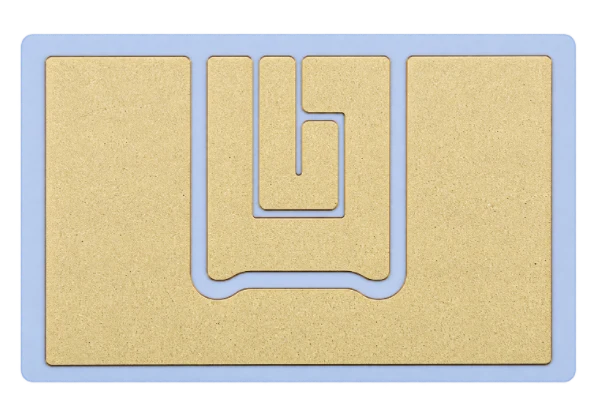
An hliníková deska plošných spojů or copper base circuit board can suit thermally concentrated LED, motor-driver and power electronics assemblies. A ceramic circuit board may instead use alumina (Al₂O₃) or aluminum nitride (AlN), depending on thermal, dielectric and mechanical requirements. Power-module DBC/AMB, precision-pattern DPC, thick-film and thin-film ceramic products are specialist construction routes, not interchangeable names for the same process.
Ceramic substrates and advanced thermal constructions
Specialized ceramic and embedded-component circuit boards can be evaluated as separate product specifications rather than assumed variants of an ordinary FR-4 PCB. Highleap has published ceramic PCB manufacturing information a DBC ceramic substrate resources for power and thermal applications. DPC, AMB, thick-film and thin-film requests require confirmation of the exact substrate and production route.
Some of these requests require specialist substrate or packaging facilities. Highleap can review the package and confirm whether the project is within its agreed manufacturing or sourcing scope.
Ceramic substrate, buried component and specialist packaging RFQs
Embedded passives are built into an engineered stack-up with an electrical acceptance plan. Embedded semiconductor die and an IC substrate belong closer to advanced packaging and demand specialist evaluation; they should not be sold as if they were routine PCB drilling options. A design using an embedded copper thermal insert is a different request from a board with an embedded capacitor or a packaged semiconductor die.
Hybrid RF/digital designs may also mix dielectric systems. Materials, compatible lamination and high-speed acceptance criteria belong in the approved cross-section before production starts.
For a ceramic PCB assembly, the supplied package should specify substrate grade, metal thickness, attachment/bonding method, hole and edge features, flatness, thermal interface and any wire-bonding requirement. Highleap can review specialist ceramic or advanced-package requests, but the exact factory route, subcontracted operations and available verification must be confirmed for the project.
RF, High-Frequency, High-Speed and Network Circuit Boards
RF circuit boards, high-frequency circuit boards and high-speed digital circuit boards can be fabricated and assembled for communications, networking, computing and measurement equipment. Příklady zahrnují 5G RF front-end PCBs, microwave sensor boards, radar modules, satellite communication circuit boards, industrial Ethernet boards, PoE network switch circuit boards, router PCBs, optical transceiver interface boards, server backplanes and high-speed connector cards.
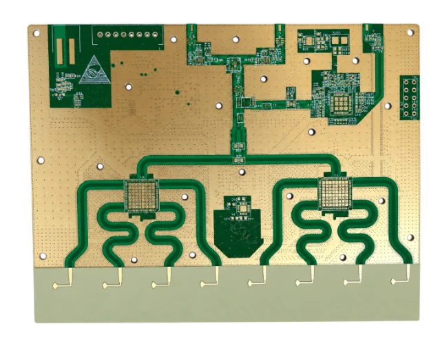
Network switch PCB, 5G module and high-speed backplane manufacturing
A network switch circuit board may use a BGA switching ASIC, Ethernet magnetics, SFP/QSFP connectors, PoE power electronics and programmed management components. A server backplane circuit board or network daughtercard may require differential-pair routing, controlled impedance, backdrilled via stubs and a specified connector geometry. The required data rate and channel-loss budget determine the stack-up and test scope, not simply whether the board is called “high speed.”
Highleap manufactures customer-specified high-frequency and high-speed circuit boards for RF electronics, networking and high-bandwidth digital equipment. Patří mezi ně RF desky plošných spojů, microwave circuit boards, desky plošných spojů s řízenou impedancí, high-speed digital circuit boards and mixed RF/digital boards with project-specific laminates and copper configurations.
A Rogers circuit board or other low-loss laminate PCB can be requested for RF front ends, radar modules and antenna interfaces. A hybrid-material circuit board combines different laminate systems within one approved stack-up, potentially placing demanding RF or high-speed channels alongside control circuitry. That construction requires material compatibility, layer registration and press-cycle assessment; a hybrid stack-up should never be changed without OEM approval. Highleap offers high-frequency PCB fabrication support for these product families.
Backdrilled high-speed circuit boards can be combined with low-loss materials, controlled copper geometry and specified connector launches for high-speed switches, optical network equipment and compute modules. Bare-board TDR can verify designated impedance coupons, while insertion loss and other channel measurements require appropriate structures and equipment. A circuit board quotation must identify which evidence is part of the standard build and which is a separate agreed measurement.
For assembled RF modules, approved matching components, soldering thermal limits, shield cans, coax interfaces and any post-assembly tuning can become as important as laminate selection. Highleap can combine board fabrication with a defined RF PCBA manufacturing package; specialized VNA, mmWave or system-level RF qualification needs explicit confirmation.
For SMT-populated RF or communication modules, Highleap can quote RF connector assembly, fine-pitch package placement, shielding and the customer-defined board-level test. TDR coupon data addresses impedance; insertion loss, return loss, RF gain, noise figure, Ethernet link performance and product EMC are separate measurements whose scope must be agreed.
Flexible, Rigid-Flex and Ultra-Thin Circuit Boards
Flexible circuit board, rigid-flex circuit board and semi-flex circuit board manufacturing are available for products whose wiring and component placement cannot be accommodated by ordinary rigid boards alone. These include camera and sensor modules, compact control devices, wearable electronics, medical instruments, folded display assemblies and cable-replacement interconnects. Highleap’s custom flexible PCB manufacturing a rigid-flex board construction can be coordinated with populated assembly requirements.
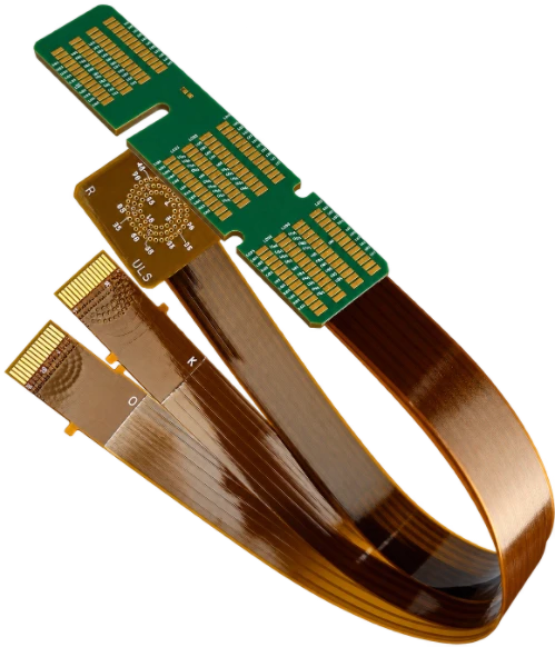
FPC keyboard connections, foldable sensor modules and multi-board wearable assemblies may use PI flex, coverlay, rigid regions and locally supported connector ends. Dynamic bend and one-time installation bend are separate specifications: copper design, bend direction, layer transitions and stiffener placement must match the intended movement.
A flex-region reinforcement is part of the finished board definition and may change soldering fixture, minimum bend radius and connector insertion.
Flexible circuit board and stiffener variants
Common variations include a single-sided flexible circuit board, double-sided flex PCB, multilayer flexible circuit board, A flex PCB with stiffener for component placement, connector insertion or screw mounting. A deska plošných spojů rigid-flex combines dedicated rigid and flexible regions without automatically requiring separate connectors. A semi-flex circuit board uses a controlled flexible region in a mainly rigid construction for applications with a defined forming requirement; it should not be treated as a substitute for repeated dynamic bending unless qualified for that duty.
Before PCBA production, define static versus dynamic flex duty, minimum bend radius, flex region keep-outs, stiffener material and thickness, coverlay access openings, assembly carrier and final fold orientation. The rigid-flex cover-opening structure described above is one specialized subcategory within this family, rather than a second name for all flexible boards.
For customers requiring populated FPCs or folded assemblies, the PCB and SMT teams need a single approved fixture/handling plan. Our rigid-flex PCB assembly support can be evaluated with the actual component placement and mechanical integration requirements.
Gold Finger and Hard Gold-Plated Circuit Boards
Gold finger circuit board manufacturing is available for pluggable products that require defined contact plating and mating geometry. Highleap's edge-card gold finger PCB capability addresses connector fingers on network cards, computing expansion boards, controller modules, industrial backplanes and removable daughtercards. The final design must match the mating socket’s board thickness, finger pitch, insertion geometry and contact finish.
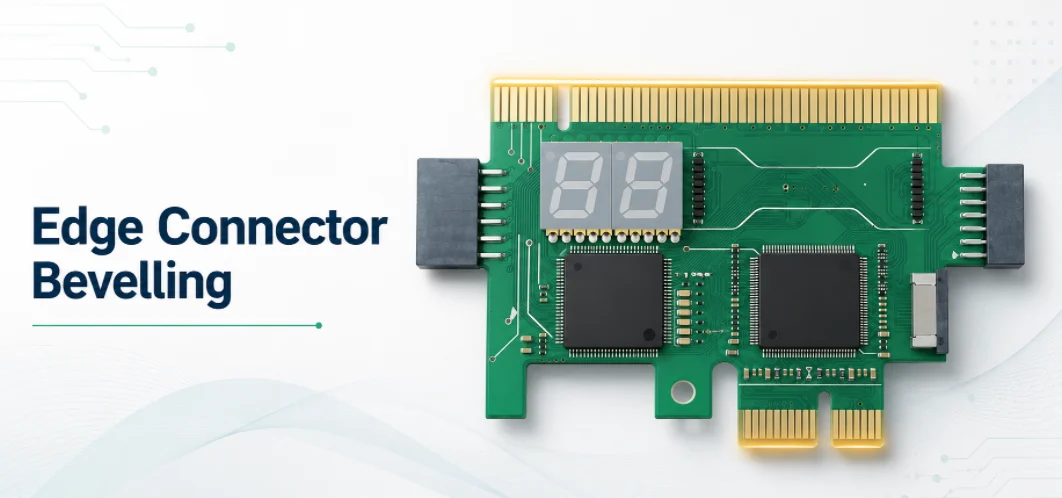
The requested gold contact structure determines how edge geometry, plating thickness and the surrounding SMT pad finish are specified. Hard gold, soft gold and immersion gold are not interchangeable for every connector or bonding application.
Gold finger PCB variations and selective plating
Gold finger PCB, beveled edge PCB and selective hard-gold circuit board
A hard gold finger PCB is normally specified for mechanical mating contacts where wear resistance matters; it should not be replaced with ordinary immersion gold merely because both finishes look gold-colored. Customers should state the nickel and gold plating system, required thickness, contact area, mating-cycle expectation and any industry-specific acceptance criteria. For a beveled gold finger circuit board, the edge chamfer angle and finished thickness must also suit the connector.
Boards requiring solderable pads elsewhere may use different finishes in different regions. A selective hard-gold and ENIG circuit board, for example, can keep wear-resistant edge contacts separate from ordinary SMT lands when the approved manufacturing route supports it. Plating-thickness evidence and finish boundaries should be agreed before production.
Edge-plated circuit board and side-plated PCB
Edge-plated circuit boards a side-plated PCBs add metal to defined board edges for grounding, contact or shielding structures. These are not the same as edge-card gold fingers: edge plating can wrap around the physical perimeter, while gold fingers are discrete contact pads on a board face. Highleap’s PCB edge metallization resources can be reviewed for RF shield interfaces, enclosure grounding and modules that require solderable sidewalls. The drawing should call out plated edge segments, interrupted areas, corner geometry and the intended connection to copper layers.
For an edge connector PCBA, we also check the keep-out zone for components, the assembly panel break-off arrangement and whether final cleaning, soldering or coating might contaminate the contact region. This connects the bare-board connector construction to a usable assembled circuit card.
ENIG, ENEPIG and Selective Surface Finish Circuit Boards
Custom circuit boards may also need surface features that cannot be described by a generic “green solder mask and immersion gold” quotation. These features change how the finished board contacts a connector, accepts solder, supports bonding or survives a downstream assembly step.
Surface finish selection must follow soldering, contact-wear and any wire-bonding requirements. The following options are quoted by location and finish specification rather than by appearance.
Surface finish options for circuit board quotations
ENEPIG circuit board and selective-finish PCB
An ENEPIG circuit board can be specified for compatible soldering and selected bonding requirements where the approved finish system is suitable. A selective surface-finish PCB may combine one finish on solder lands with another on electrical contacts, but the selective areas and finish thicknesses must be identified on the drawing. The ENEPIG PCB finish option is part of the broader special-board manufacturing discussion. Neither ENEPIG nor ENIG should automatically be treated as equivalent to electrolytic hard gold for high-wear edge connectors.
For these nonstandard board finishes, the fabrication notes should say which areas are to be soldered, plugged in, bonded, contacted or temporarily protected. The final surface configuration has to be compatible with the OEM’s assembly sequence, not chosen solely from the lowest-cost finish option.
HDI, Blind/Buried Via and Filled-Via Circuit Boards
Highleap manufactures advanced interconnect circuit boards for designs where standard through-via fan-out is insufficient. Náš HDI circuit board manufacturing scope supports discussions of fine-line routing, microvias, multi-stage lamination and the component-land arrangements needed by compact processors, memory and communication devices.
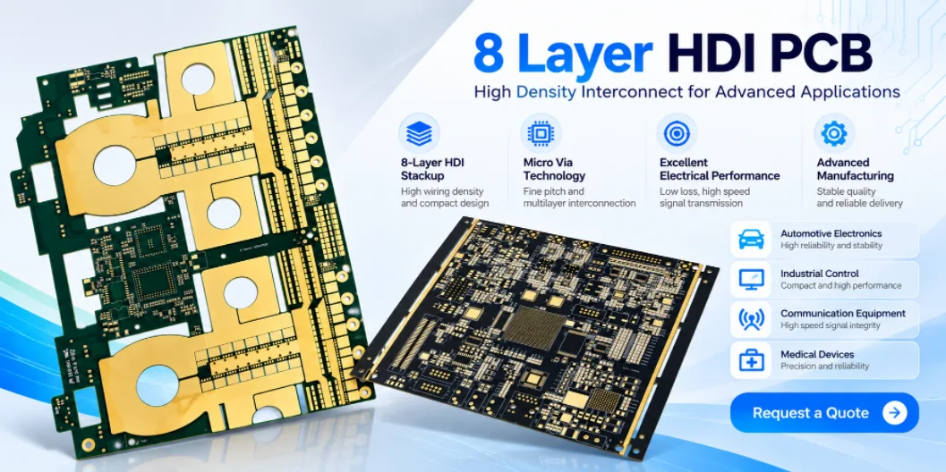
Vias are not described correctly by hole diameter alone. Their layer span, filling, cap plating and final solder-pad function determine both bare-board feasibility and assembly yield.
HDI via structures and termination choices
Blind-via, buried-via, stacked-microvia and staggered-microvia PCBs
Blind-via circuit boards connect an outer layer to specified inner layers without extending through the entire PCB; buried-via circuit boards connect internal layers without openings on the finished surfaces. Stacked microvia PCBs a staggered microvia boards use different microvia arrangements to reach required layers. They must be assessed against the laminate and via-reliability requirements rather than described as interchangeable HDI options. Designs requesting any-layer interconnect HDI PCBs require an even more specific stack-up and feasibility review.
Via-in-pad, resin-filled, copper-capped and backdrilled circuit boards
A via-in-pad circuit board can route signals out of fine-pitch BGA or chip-scale packages, but open vias under solder lands may drain solder or create void-related concerns. For the specified packages, a resin-filled via PCB with planarization and copper capping may be requested to create a usable assembly land. These are different requirements from simply tenting a via with solder mask. Highleap’s via-in-pad construction guidance is relevant to defining the feature before fabrication.
For servers, network switches, high-speed interface cards and some RF systems, a backdrilled circuit board removes selected unused portions of plated through-via barrels. Backdrilling requires defined entry direction, target layer, residual-stub allowance and clearance from active connections. It does not by itself establish finished channel loss or signal performance; those require the appropriate customer acceptance plan.
These HDI choices should be finalized alongside the BGA ball map, via fill requirement, inspection plan and board-to-assembly handoff. The stejný HDI Gerber set cannot be priced accurately if the build instructions alternately call for open, plugged and filled/capped vias.
SPECIAL-FEATURE REVIEW
Combining HDI with other special features?
Share your stack-up, fabrication drawing and feature requirements. We can review feasibility, inspection needs and quotation details before production.
Castellated, Edge-Plated and Special-Hole Circuit Boards
Highleap can evaluate circuit boards with specialized edge terminals, plated slots and mechanical mounting holes as part of the finished PCB definition. These requirements are particularly relevant to RF modules, industrial controls, power supplies and electronics that must solder or fasten into another assembly.

These features are mechanical/electrical interfaces in the finished PCB. A finished-hole dimension, plated-edge drawing or module carrier footprint is more useful than a broad “special hole” request.
Board edges, castellations, slots and mounting-hole variations
Castellated-hole PCB and plated half-hole circuit board
A castellated circuit board uses metallized half-holes at the perimeter so that a module can be soldered onto a carrier board. Common products include Wi-Fi/Bluetooth modules, GNSS receiver modules, sensor daughtercards and compact control units. Highleap’s castellated module PCB manufacturing guidance covers this structural family. Hole location relative to routing, barrel integrity, surface finish and the carrier board footprint all need to be compatible. A plated half-hole PCB is often specified by essentially the same terminal construction; it is not counted as a separate soldering technology in the quote.
Plated slot PCB, press-fit PCB and countersunk-hole PCB
Plated slot circuit boards provide elongated conductive openings for connector blades, shield tabs and mechanical/electrical terminals. Non-plated routed-slot PCBs instead provide mechanical clearance or isolation slots. The routed width, finished plating, tolerances and solder-mask clearance are different, so the two drawings should never be assumed equivalent.
Press-fit connector circuit boards require finished-hole diameter and plating specifications matched to the connector manufacturer’s compliant-pin requirements. A through-hole pad that works for wave soldering does not necessarily satisfy press-fit insertion forces or retention. For a countersunk PCB or counterbored circuit board, the fastener head or mounting boss also determines the depth, diameter, side of entry and remaining laminate thickness. Highleap documents countersink and counterbore PCB features for these mechanical interfaces.
The most useful RFQ includes the mating part and finished-hole or finished-slot requirements, not only a Gerber image of an unusual shape. Mechanical acceptance affects both PCB manufacturing and the subsequent assembly fixture.
Cavity, Stepped and Controlled-Depth Circuit Boards
Recessed-cavity, controlled-depth and open-cover circuit boards are different special constructions that must be quoted by the exact cross-section. They are used to manage package height, reveal selected internal regions or create exposed flex sections where the board must fold inside a product enclosure.
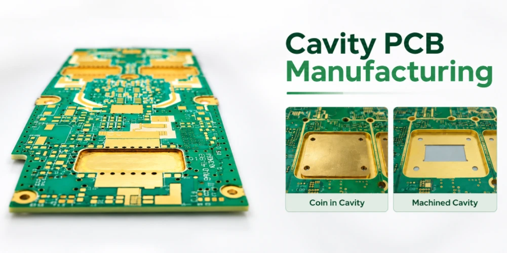
A rigid-board cavity is not the same as a rigid-flex cover-removal window. Each requires its own cross-section and final exposed-area specification.
Recessed, stepped and depth-controlled PCB structures
Cavity PCB and controlled-depth milled circuit board
A cavity circuit board has a defined recess or pocket in the finished construction, potentially accommodating a component, thermal feature or mechanical interface. A controlled-depth milled PCB or recessed pocket PCB specifies the remaining dielectric/copper clearance underneath an area that is not fully routed through the board. These designs need the pocket outline, depth reference surface, flatness, allowed substrate exposure and any copper keep-outs called out in the fabrication drawing. If a pocket exposes copper, its required finish and protection must also be defined.
Pro stepped-thickness PCB or step-milled circuit board, different board regions have different final thicknesses. That can support connectors and mechanical fit in compact equipment, but it introduces dimensional and lamination constraints that vary by design. Depth-controlled routing is not the same as a generic external board profile.
Rigid-flex PCB cover opening and cap-removal circuit board
In rigid-flex manufacturing, a cover-opening PCB or rigid-flex cover-removal board refers to removing the specified rigid-layer cap over a flexible region so the intended flex window is exposed. It is a different structure from a recess milled into a rigid cavity PCB. The flex core, coverlay, window shape, rigid-to-flex boundary, bonding material and final fold path must be controlled together. A PCB order described only as “open cover” is incomplete unless the cross-section and exact removal layers are supplied.
Highleap’s custom rigid-flex circuit board manufacturing offers a relevant engineering starting point for this board family. Specific cover opening, laser or depth-routed cap removal and special cavity feasibility are subject to the released layer structure and production assessment. We do not assume every possible open-cover construction is available without design review.
Carbon Ink, Special Solder Mask and Panelized Circuit Boards
Custom carbon patterns, special solder-mask openings and production markings can be specified as functional features of a finished circuit board. A carbon keypad contact needs measurable electrical and wear performance; a selective solder-mask opening needs an accurate mask drawing; serialized laser or ink marking needs a legible encoding and location. These are not interchangeable decorative options.
Markings, special ink and mask constraints should be captured in separate artwork layers, not inferred from a product photograph.
Printed conductive ink, solder-mask and traceability features
For industrial modules and serviceable electronics, the marking scheme may link the bare-board lot to the finished PCBA serial record. Highleap can review peelable mask requirements alongside the assembly and packaging stage at which the protection is removed.
Panelized and precision-routed circuit boards
Panel format is part of the PCB product quotation when special board geometry must survive SMT assembly and controlled depanelization. Complex contours, tabs, V-score interruptions and custom tooling edges affect stencil support, placement, soldering fixtures and post-assembly breakout.
Choose panel geometry with the planned SMT line and component-edge clearances in mind.
PCB routing, scoring and panelization variants
An industrial module panel containing several board revisions needs an approved panel map and identification scheme. A mixed-board panel is not automatically the lowest-cost option: tooling, electrical test, placement program and traceability can offset material savings.
Turnkey Circuit Board Assembly, Programming and Box Build
Highleap’s one-stop circuit board service can extend from finished bare PCBs to fully populated PCB assemblies and defined electromechanical builds. The factory-coordinated scope can include bare board fabrication, approved electronic component procurement, stencil preparation, SMT placement, through-hole insertion, inspection, IC programming, functional testing, coating, harnessing and enclosure integration according to the signed manufacturing package.
A keyboard project may require PCB, switch sockets, MCU programming, RGB LED placement, connectors and case integration. An LED lighting project may require metal-core LED modules plus a separate driver PCB and cable set. An inverter may include a gate-driver board, power control board, communication board and a display. Each finished set needs its own BOM, assembly drawing and test definition.
Highleap can supply custom boards as populated circuit board assemblies, allowing the special PCB construction and its assembly requirements to be reviewed in one project. Náš SMT and through-hole circuit board assembly services address fine-pitch components, QFNs, BGAs, connectors, relays, power devices and mechanical hardware subject to the released manufacturing specification.
The following requests belong to the agreed assembled-board or post-fabrication scope. Coating, potting, underfill and ESD performance must never be treated as interchangeable quality claims.
Post-assembly protection, cleanliness and encapsulation
Special boards need special attention at assembly. A gold-finger card needs contact protection and a compatible panel arrangement; a castellated RF module must have solderable edge terminals; a cavity board may need a stencil or fixture adapted to different surface heights; a rigid-flex board may require carriers and support for the flexible sections; heavy-copper power boards can require different soldering considerations from fine-pitch control areas on the same PCB.
For OEM programs containing several boards, we can coordinate the power board, control board, interface card and communication module as related part numbers while retaining their individual revisions and test criteria. The manufacturing scope identifies which operations and documents are included; not every advanced PCB construction or laboratory test is automatically available within the same physical factory.
Circuit Board Prototypes, Inspection and Quality Assurance
Highleap can quote special circuit board prototypes and repeat manufacturing with inspection evidence matched to the feature being purchased. A prototype circuit board manufacturing project may establish a gold-finger fit, cavity profile, HDI via cross-section, flex-bend geometry or copper-insert interface before a larger order is released. The production objective should be stated up front so that the prototype proves the correct feature.
For bare boards, electrical continuity/isolation testing is complemented by feature-specific checks when required: gold-plating thickness and bevel geometry for edge contacts; plated-hole or slot dimensions for connector boards; step depth and remaining laminate thickness for cavity boards; microsection and filled-via condition for HDI boards; and material/stack-up data for controlled-impedance constructions. Inspection records and sampling frequency are defined in the project quality plan.
After component assembly, AOI, X-ray where appropriate and the customer’s functional test address different aspects of workmanship and performance. Highleap’s PCBA functional testing services can be specified for power rails, digital interfaces, programmed configuration or other application-defined checks. TDR impedance measurements do not independently prove RF insertion loss, and a normal functional test does not replace humidity, thermal cycling or regulatory certification.
Production releases should identify the board part number, revision, material and special feature drawing, surface finish, approved component list, expected test evidence and any independent testing requirement. This keeps a complex special-feature board reproducible between prototypes and volume orders.
Circuit Board Quote, Cost and Special-Feature RFQ
For a circuit board manufacturing quotation, send Highleap the feature-specific fabrication package rather than only a picture or a generic “complex PCB” description. We can review bare PCB, PCB assembly or complete turnkey requests and identify any technical questions before pricing, tooling and material commitments are finalized.
- Údaje o desce plošných spojů: Gerber/ODB++ or equivalent, drill/rout files, fabrication drawing, complete stack-up, substrate and surface finish.
- Special feature instructions: gold finger plating and bevel; castellated edge/slot details; cavity or step depth; rigid-flex cover-removal zones; finished press-fit or countersunk dimensions; via fill, backdrill and buried-via definitions.
- Electrical and thermal requirements: controlled impedance, insertion-loss or RF test scope, current paths, thermal inserts, dielectric isolation, mounting and mechanical interface dimensions.
- Assembly package, if required: BOM with approved manufacturer part numbers, CPL/centroid, assembly drawings, software programming files, inspection criteria and functional-test procedure.
- Rozsah objednávky: prototype quantity, expected annual volume, requested shipment date, delivery destination, quality documentation and any specialist or third-party process requirement.
Can Highleap manufacture a circuit board with more than one special feature? Yes, such combinations can be evaluated during engineering review—for example, a multilayer gold-finger PCB with backdrilled high-speed channels, an HDI rigid-flex PCB with exposed flex windows, or a copper-insert power board with SMT control electronics. Final availability, tolerances, materials and test scope depend on the complete released design.
Can Highleap deliver the populated assembly as well as the bare board? Yes. PCB fabrication, electronic component sourcing and PCBA can be coordinated under one commercial project, with specialist features and the relevant manufacturing or inspection responsibilities stated in the quotation.
Manufacturing scope note: Standard and special-feature PCB requirements are subject to engineering feasibility, material availability, tooling, drawing tolerances, and the agreed production/testing route. Mention of a construction or industry in this article is not an unconditional promise of in-house processing or finished-product regulatory certification.
READY FOR A QUOTATION
Request a PCB manufacturing and assembly quote
Use the checklist above to describe your board, special features, quantity and assembly needs. Start with the inquiry form and our team will follow up about your project.
doporučené příspěvky

Výrobce osazování desek plošných spojů v Číně
Highleap Electronics je výrobce desek plošných spojů v...

Sestavení plošných spojů síťového přepínače: Testování Ethernetu, PoE a portů
Osazování desek plošných spojů síťových přepínačů ve společnosti Highleap Electronics přináší...

Sestava plošných spojů výkonové elektroniky pro systémy s vysokým proudem a převodem energie
Highleap Electronics dodává desky plošných spojů pro výkonovou elektroniku...

Osazování automobilové elektroniky na plošných spojích: Sledovatelnost a řízení procesů
Highleap Electronics vyrábí desky plošných spojů a dodává...
Jak získat cenovou nabídku na desky plošných spojů
Provedeme pro vás analýzu DFM/DFA a ozveme se vám se zprávou. Své soubory můžete bezpečně nahrát prostřednictvím našich webových stránek. Pro vypracování cenové nabídky potřebujeme následující informace:
-
- Gerber, ODB++ nebo .pcb, spec.
- Seznam kusovníků, pokud požadujete montáž
- Množství
- Čas otáčení
Kromě výroby desek plošných spojů nabízíme komplexní škálu elektronických služeb, včetně návrhu desek plošných spojů, výroby desek plošných spojů a komplexních řešení. Ať už potřebujete pomoc s prototypováním, ověřováním návrhu, zajištěním zdrojů součástek nebo hromadnou výrobou, poskytujeme komplexní podporu, abychom zajistili úspěch vašeho projektu.
Pro služby PCBA prosím poskytněte kusovník (BOM) a případné konkrétní montážní pokyny. Nabízíme také analýzy DFM/DFA pro optimalizaci vašich návrhů z hlediska vyrobitelnosti a montáže a zajištění plynulého výrobního procesu.