
IT-858G Placas de Circuito Impresso Automotivas para Controle de Potência com Alta Densidade de Cobre
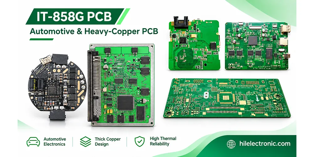
IT-858G PCB applications in automotive electronics and heavy-copper power-control designs.
Automotive ECU and power-control boards often combine heavy copper, high thermal loading and closely spaced plated features. IT-858G is a high-Tg, halogen-free filled-epoxy material option used in this type of design; its CAF and thermal data must be interpreted separately from finished-board voltage ratings and qualification. For IT-858G projects, Highleap can support PCB fabrication and assembly review around copper weight, resin fill, hole-wall plating, insulation spacing and SMT or through-hole component requirements.
IT-858G is specified for its 200°C Tg (DSC), low Z-axis expansion and manufacturer-reported CAF resistance. These properties are relevant to plated-through-hole fatigue and insulation reliability, but a supplier CAF test at 1000 V is not a 1000 V operating-voltage certification for a fabricated or assembled board.
What IT-858G Provides—and What a 1,000 V CAF Claim Does Not Mean
Material CAF resistance and system insulation are separate calculations
If two plated holes carry different voltages, the shortest physical distance between their conductive surfaces is not necessarily the entire insulation story. The hole-wall finish, resin/glass interface, moisture penetration path, contaminant residues and electric-field concentration determine where degradation can begin. Internal CAF evaluation commonly uses defined test coupons and biased humidity conditions, while product isolation must consider the actual operating voltage, applicable safety standard and assembly environment. The supplier’s stated 1,000 V resistance cannot be converted into an allowable 1,000 V working voltage without the missing geometry and test details.
Nor should a CTI category of 250–399 V be described as a maximum service voltage. CTI is a standardized surface tracking classification. A completed PCB may require a different creepage or clearance than the base material classification alone suggests, particularly when coating, altitude, pollution degree or transient overvoltage is relevant.
The current IT-858G supplier datasheet identifies a multifunctional filled-epoxy system with 200°C Tg by DSC, 1.4% Z-axis expansion from 50°C to 260°C and a 5%-weight-loss decomposition temperature of 395°C. It also references CAF resistance at 1,000 V and through-hole reliability. These are useful screening properties, but the 1,000 V statement is not equivalent to approving any finished PCB for 1,000 V continuous service.
| Propriedade publicada | IT-858G typical | Proper engineering interpretation |
|---|---|---|
| Tg | 200°C, DSC | A material transition result; not a continuous-use temperature rating |
| Thermal resistance, T288 | Mais de 60 minutos | Specific supplier test result; not a soldering process recipe |
| Expansão no eixo Z, 50–260°C | 1.4% | One input to plated-hole thermal-fatigue risk |
| CTE X/Y, 40–125°C | 12 / 13 ppm/°C | Relevant to registration and component/board expansion mismatch |
| Dk / Df at 10 GHz, 50% resin | 4.67 / 0.014 | A standard-loss rather than ultra-low-loss electrical profile |
| CTI category | CTI 2, 250–399 V | Surface tracking classification; not an assembly isolation voltage |
| CAF | Supplier reports 1,000 V resistance | Must be interpreted with the original test configuration and bias/environment |
A distinção entre CAF e CTI is important. Conductive anodic filamentation develops along susceptible internal glass/resin interfaces under moisture and electrical bias. Tracking index addresses surface tracking under a standardized test. Neither test alone establishes creepage/clearance compliance, dielectric withstand or the qualification of a specific electronic control unit. For finished boards, the important variables include hole-to-hole distance, drill quality, cleanliness, conductor geometry and the agreed humidity/bias environment.
IT-858G is therefore better positioned as a high-reliability standard-loss substrate than as a high-speed channel-loss solution. Choosing it for a power/ECU board on the basis of insulation, thermal or plated-hole needs is a different decision from selecting a very-low-Df laminate for an optical switch.
High-Tg PCB material selection for automotive power-control electronics
IT-858G belongs to a different purchase decision than an ultra-low-loss switch laminate. An automotive ECU PCB manufacturer evaluates a high-Tg filled-epoxy material against heat exposure, plated-hole geometry, moisture and bias conditions, copper weight and the application’s own qualification requirements. The supplier’s material CAF result is relevant, but it does not replace automotive validation or a creepage-and-clearance review.
For a power-control board, the procurement drawing should name the required laminate and prepreg, finished copper thickness, minimum dielectric spacing, via/hole details and IPC workmanship requirements. A fabricator cannot promise a finished-board insulation rating solely from the material’s published CAF or CTI information.
Heavy-Copper Automotive ECU PCB Stack-Up with IT-858G
Dielectric thickness can fail locally while average board thickness looks correct
A global thickness check may show a board within specification even though resin has flowed away from the crest of a tall copper trace. The critical dimension for dielectric withstand can be the minimum local resin-and-glass separation at the edge of that feature. Resin-rich pockets and glass-displacement zones can coexist on the same cross-section. The stack-up should therefore define where thickness is measured and how the minimum dielectric barrier is accepted, particularly if copper weights or pattern density differ sharply between adjacent layers.
O heat-spreading paths created by thick copper planes and thermal-via arrays should also be evaluated with the mechanical mounting scheme: a high-power component above an uneven copper region can concentrate temperature and assembly stress. More copper improves conduction only when a continuous path to the heat sink or chassis exists.
Heavy copper changes more than current-carrying capacity. A thick etched feature leaves a deep topographic cavity next to it, and the prepreg must supply enough resin to fill that volume while retaining the required dielectric thickness over the top of the copper. Poor resin balance can produce voids, locally thinned insulation or interlayer separations even when the material passes standard thermal tests.
Finished trace width and minimum spacing should be checked against thick-copper etching and sidewall compensation rules, because copper weight changes side-etch behavior and the finished conductor profile.
A suitable heavy-copper construction must define copper balance and pressed dielectric spacing across power layers by specifying the copper weight per layer, copper-free fields, adjacent plane density and target insulation thickness. The press construction must be calculated from the actual copper pattern, not a nominal prepreg thickness alone.
Why the copper area fraction affects the press result
Considere um cálculo ilustrativo, not a production claim: a 100 mm × 100 mm layer with 70 µm copper and 40% etched-open area has a gross open-feature volume of 100 × 100 × 0.07 × 0.40 = 280 mm³. The actual resin requirement differs because nearby features, glass, resin squeeze-out and the adjacent layer also consume or redistribute material. Still, this estimate shows why both copper thickness and open-area percentage belong in the lamination review.
For boards carrying substantial current, PCB thermal-management techniques also need to account for copper planes, thermal vias, component heat paths, mounting features and air flow. A laminate’s thermal characteristics do not independently predict the hottest component temperature. Equally, substituting thick copper for thermal vias may alter current distribution and compromise assembly flatness.
The review should separate three acceptance targets: minimum finished dielectric thickness, minimum copper thickness after etch/plating and acceptable voiding or delamination. Those values should appear in the fabrication drawing or project specification rather than being inferred from IT-858G’s Tg.
Heavy-copper PCB fabrication: why resin fill and dielectric spacing are connected
In a thick-copper power PCB, tall etched traces consume resin volume during pressing. The most important dielectric dimension can be the local separation above a conductor corner rather than the average finished board thickness. Copper-fill percentage also varies by layer: a large solid power plane and a sparse control layer do not demand resin in the same way.
The prepreg construction therefore needs to be evaluated together with copper weight, etched pattern density, target pressed thickness and the specified electrical isolation. Representative microsections can show resin starvation, voids or insufficient separation in the same locations where a simplified stack-up drawing appears satisfactory.
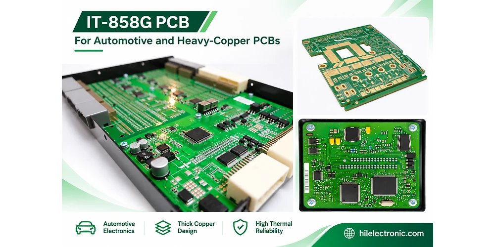
Board construction and assembly examples for the IT-858G heavy-copper manufacturing review.
CAF Resistance, Drilled-Hole Quality and Plated-Through-Hole Fatigue
The path to a reliable multilayer high-voltage board runs through the hole wall. Drilling can generate glass-fiber disturbance, resin smear and mechanically damaged interfaces. If these remain after hole preparation, copper metallization may not bond uniformly; discontinuities can then become both an electrical and moisture-related reliability risk.
Two distinct failure routes require different evidence
| Modo de falha | Mecanismo físico | Inspection or qualification evidence |
|---|---|---|
| Plated-through-hole barrel crack | Z-axis expansion cyclically strains copper, often near the knee or interface | Representative microsections and specified thermal-stress/cycling tests |
| Conductive anodic filament | Moisture and electric field support an internal conductive path along a susceptible interface | Design-representative spacing, contamination controls and biased-humidity testing when specified |
| Interlayer void near thick copper | Resin demand exceeds local filling capability or press consolidation is inadequate | Pressed-stack microsection and dielectric thickness measurements |
| Insulation breakdown or surface tracking | Excessive local field, inadequate geometry or contamination | Specified dielectric test plus appropriate creepage/clearance analysis |
The design of a material system that resists CAF growth under moisture, temperature and electrical bias is inseparable from drilling and fabrication cleanliness. The supplier’s 1,000 V material claim does not establish a finished-board operating voltage; qualification must use the actual conductor spacing and the specified humidity/bias conditions.
The drilling route must account for board thickness, drill diameter, feed and tool wear, particularly where thick copper and dense via fields are present. Hole preparation then requires effective smear removal without damaging resin/glass interfaces. Microsections should examine barrel coverage, internal-layer connections and resin recession. The plating control for high-current via barrels and thick-copper features becomes especially important where aspect ratio and current density make copper distribution difficult.
The central reliability distinction is that published low Z-axis expansion reduces one contributor to dielectric strain on the copper barrel, but only adequate barrel copper and sound interfaces make that benefit useful. The thermal-stress qualification of thick-copper constructions should therefore reflect the specified copper weight, hole geometry and assembly/service temperature profile.
FABRICAÇÃO E MONTAGEM DE PCBs
Developing an IT-858G automotive or power-control PCB?
Highleap can discuss copper weight, plated-hole requirements and the intended SMT or through-hole assembly scope for the board.
Uma primeira consulta é simples. No full drawing set is needed to begin. Start with the board’s application and approximate quantity; copper-weight and reliability details can be added during engineering review.
Automotive ECU PCB Manufacturing: Inspection and Thermal Reliability
Automotive electronics involve multiple qualification boundaries. IT-858G’s data may support a board-material proposal, but an ECU’s lifetime requirements depend on defined temperature cycling, vibration, humidity, electrical bias and assembly design. The automotive board design constraints for thermal and vibration environments should be translated into the fabrication and qualification requirements rather than reduced to a generic “automotive grade” description.
A practical sequence starts with material callout and stack-up approval, continues through copper balance and lamination evidence, then confirms hole quality and electrical tests. For higher-reliability applications, the project owner may require additional thermal cycling, CAF/SIR, cleanliness or dielectric-strength testing on representative coupon designs. The scope and pass/fail criteria must be agreed before the build.
Key control points for an IT-858G fabrication route:
- Confirm the exact laminate and prepreg designations, foil type, pressed dielectric targets and substitution approval rules.
- Review resin sufficiency around thick copper, as described by the relationship between PCB resin content and etched copper distribution.
- Record drill-wall quality and copper plating integrity at critical hole aspect ratios and copper-to-hole intersections.
- Apply the requested IPC-6012 and IPC-A-600 acceptance criteria to the completed bare boards rather than treating the material datasheet as a board certificate.
- Define which PCB reliability tests are qualification tests and which belong to routine production acceptance.
From IT-858G Bare Boards to Lead-Free PCB Assembly
Thermal mass changes the reflow process window
A dense power plane absorbs and redistributes heat differently from a lightly populated signal region. The assembly profile must achieve adequate soldering temperatures at high-thermal-mass joints without overheating sensitive components or overexposing the laminate. That balance is established by product-specific thermocouple profiling and approved solder materials, not by copying a laminate T288 test into the oven recipe.
Rework deserves separate attention. A localized hot-air operation may generate a steeper thermal gradient than the initial reflow, especially near power connectors and large exposed pads. If the product is expected to undergo repeated repair, the acceptable rework count, inspection criteria and any post-rework electrical/thermal tests should be specified during the manufacturing planning stage.
Lead-free reflow can expose a board to temperatures well above its intended operating range. A 200°C Tg does not authorize unrestricted peak temperature or repeated rework. The solder paste, board thermal mass, component limits and actual product profile govern the assembly process. Large copper planes can create local thermal gradients and make solder-joint formation harder to balance across the board.
When an IT-858G design includes press-fit pins, high-current terminals, power packages or heat-intensive joints, solder-joint planning around high-current terminals and power packages should be coordinated with the approved bare-board construction. Where required by the assembly plan, wetting verification for pads and plated through-holes can help assess finished-surface condition before assembly.
At production transfer, first-article checks for placement, polarity and solder-joint workmanship can compare populated boards with the released assembly package. These inspections complement—not replace—the laminate, hole-wall and insulation evidence required for the bare PCB.
During detailed engineering review, Highleap can evaluate the IT-858G material specification, heavy-copper construction, spacing rules, plated-hole design, assembly scope and requested testing. The drawing and test requirements are checked against the actual board construction; any special qualification is established from the project requirements rather than assumed from the material name.
Lead-free automotive PCBA with heavy copper and mixed thermal mass
Heavy-copper power-control assemblies may combine large MOSFET pads, connectors and small signal components. A single reflow profile must create adequate solder joints without exceeding component or laminate temperature limits; high thermal mass can make the process window narrower. Board flatness, solder-mask definition, thermal pad geometry and post-assembly inspection deserve attention before transferring a bare-board qualification into production PCBA.
Before production release, the assembly data and agreed test requirements should be checked against the IT-858G bare-board construction and the actual component set. That coordination belongs to the engineering handoff; it does not need to delay an initial supplier discussion.

Sobre o autor
Carlos L
Engenheiro de CAM e Manufatura de PCB na Highleap Electronics
Charles possui mais de 10 anos de experiência em engenharia CAM de PCBs e fabricação eletrônica, com especialização em verificação de arquivos de PCB, análise DFM e preparação para produção de placas multicamadas, HDI, RF e de alta velocidade. Proficiente em Genesis, InCAM e CAM350, ele garante dados precisos, processos estáveis e alto rendimento de fabricação.
Na Highleap Electronics, ele se concentra na otimização de processos e na avaliação da viabilidade de fabricação para ajudar os clientes a reduzir riscos, diminuir prazos de entrega e alcançar resultados de produção confiáveis.

Posts recomendados
Placa de circuito impresso Arlon 85NT: Fabricação em poliimida e controle SMT
Ilustração da fabricação de PCBs; grau do material e...
Fabricação de PCBs Arlon 33N de alta qualidade
Ilustração para fabricação de PCB. Confirme as especificações...
Fabricação de PCBs Arlon 35N e Laminação de Poliimida
Ilustração para fabricação de PCB. Confirme as especificações...
Fabricação de PCBs Arlon 45NK de baixo CTE na China
Ilustração para fabricação de PCB. Confirme as especificações...
Como obter um orçamento para PCBs
Vamos realizar uma análise DFM/DFA para você e entraremos em contato com um relatório. Você pode enviar seus arquivos com segurança pelo nosso site. Precisamos das seguintes informações para lhe fornecer um orçamento:
-
- Gerber, ODB++ ou .pcb, especificação.
- Lista de materiais caso necessite de montagem
- Qtd.
- Hora de virar
Além da fabricação de PCBs, oferecemos uma gama completa de serviços eletrônicos, incluindo design de PCBs, PCBA e soluções completas. Seja para prototipagem, verificação de design, fornecimento de componentes ou produção em massa, oferecemos suporte completo para garantir o sucesso do seu projeto.
Para serviços de PCBA, forneça sua BOM (Lista de Materiais) e quaisquer instruções específicas de montagem. Também oferecemos análise DFM/DFA para otimizar seus projetos quanto à capacidade de fabricação e montagem, garantindo um processo de produção tranquilo.