
NPI / PROTOTYPE PRODUCTION
Fabricarea prototipului PCB cu 14 straturi, timpul de livrare și inspecția
A 14 layer PCB prototype should validate the construction that will be carried into pilot and repeat production. Highleap Electronics coordinates multilayer fabrication reviews for engineering samples and controlled production releases, including the stackup, laminate, interconnects, inspection criteria and delivery requirements. For equipment with dense BGA routing or high-speed interfaces, a passing first board is useful only when the underlying construction and acceptance results are recorded.
Trimiteți fișierele Gerber sau ODB++, stivuirea, cantitatea țintă și cerințele de inspecție. Adăugați lista de materiale pentru asamblare.
14 Layer PCB Prototype Manufacturing and Pre-Production DFM
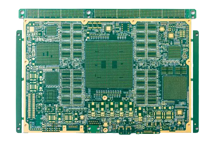
Highleap can review a fourteen-layer engineering prototype against the intended production architecture. The first sample should not be approved solely because the board powers on or passes a flying-probe test. For a high-layer-count PCB, the physical stack, via construction, laminate and controlled-impedance features affect whether the sample represents the future production product. The first order should therefore identify which parameters must remain unchanged during pilot and recurring manufacture. The approved fourteen-layer stackup and controlled-impedance review provides the physical baseline for that decision.
An effective prototype release package includes:
- Datele consiliului de administrație: all 14 copper layers, drill/slot files, finished outline, IPC-2581/ODB++ or equivalent CAM data and a drawing revision.
- Manufacturing construction: dielectric material and supplier grade or permitted substitutions, layer order, finished thickness, copper-by-layer and special via-span map.
- Electrical constraints: target impedances by reference layer, trace widths/spacings that cannot be altered without approval, and any channel loss requirement.
- Inspection and reliability: applicable rigid-board class, acceptance criteria, netlist and coupon requirements, extra microsections or sample-based stress tests as necessary.
- Assembly interface: solder finish, test-point access, BGA escape, connector hole tolerances, panel rails and intended reflow profile when a PCBA build will follow.
Highleap’s published multilayer fabrication capability information demonstrates the company’s stated broad technology range, but final feasibility is decided at the board level. The prototype order should make the production-representative requirements explicit rather than relying on generalized minimum-hole or minimum-trace figures.
Can a 14-layer PCB be prototyped using a substitute laminate?
Only if the OEM approves the difference and understands what the prototype will and will not validate. A stock material may be practical for mechanical fit, but a dielectric substitution can change controlled impedance, insertion loss, thermal expansion or via reliability. If the sample is intended to qualify a production build, using the final approved material is generally the stronger route.
Which DFM checks must be closed before the first build?
Highleap reviews the manufacturing package before the first artwork release. The data should include fourteen copper layers in the correct order, drill and slot data, finished board thickness, controlled-impedance specification, selected laminate, surface finish and any separate drawings for backdrilled or filled vias. The engineering review identifies manufacturing conflicts and proposed corrections for customer approval.
A high-layer-count rigid PCB presents combined constraints. A fine mechanical drill becomes more challenging as finished thickness grows; heavy copper affects etching and resin flow; a dense BGA can dictate escape-via geometry; and mixed low-loss dielectrics may affect lamination. No single universal design-rule table covers every combination. Highleap can use its Procesul de revizuire a DFM-ului PCB to determine the build route for the actual files.
Can a fourteen-layer design be prototyped without changing the production stackup?
Yes, when the requested material and construction are compatible with prototype volume and the target production process. Highleap can quote the same approved layer sequence, dielectric system, finished copper and via structures for the sample lot. If the prototype must use an alternative material or different process, the difference should be documented and evaluated before the engineering board is used to qualify the final product.
14 Layer PCB Lead Time, Materials and Schedule Planning
The delivery plan starts when the manufacturing package is technically released, not when an informal inquiry first arrives. Material selection, engineering questions, panel nesting, lamination stages and outsourced specialist operations can each control the schedule. A conventional PTH build on stocked material may follow a different path from a custom low-loss HDI stack with several drilling and filling operations.
| Bornă | What needs to be accepted | Schedule consequence |
|---|---|---|
| RFQ/DFM closure | Stackup, artwork, drill, inspection and allowed exceptions | Fabrication cannot be safely released with unresolved specifications |
| Material reservation | Approved laminate/foil and confirmed substitutes if any | Special grade or thickness may become the critical path |
| Multilayer core/press routing | Inner-layer processing, AOI, registration and lamination | Different via architectures may add operations |
| Drilling, plating and specialty processes | Finished hole, backdrill, VIPPO, finish and dimensional controls | More specialized processes require appropriate time and validation |
| Final acceptance and shipment | E-test, any impedance/cross-section data, packing and logistics | Reports and freight must be part of the requested arrival date |
A meaningful quote can distinguish engineering approval date, planned fabrication completion, test/report release and ex-works or delivered shipment date. Urgent orders should be evaluated against the approved materials and actual factory loading. No blanket “24-hour fourteen-layer PCB” claim is appropriate for all structures.
Can Highleap reserve material for repeated 14-layer PCB orders?
Material planning can be discussed for programs with a forecast, fixed approved grade and commercial commitment. Whether stock can be reserved depends on the specific laminate, minimum buy, agreed order releases and ownership of unused stock. A material plan should name who authorizes substitutions and who is responsible for any obsolete or excess inventory.
How does laminate procurement affect prototype lead time?
The delivery schedule starts after technical release and the necessary materials are available. A standard through-hole fourteen-layer build using stocked materials can follow a different production timeline from a stack with controlled-depth drilling, buried vias, a special low-loss laminate or additional coupons. Lamination, drill and plating capacity, inspection work and packing also affect the manufacturing window.
Highleap prepares project-specific lead-time estimates rather than applying turnaround figures for simpler PCB types to every fourteen-layer design. The requested ship date should be accompanied by the location, quantity, material restrictions and the time needed for acceptance reports. General PCB fabrication lead-time considerations explain the same dependencies across other layer counts.
Does a “quick-turn” 14-layer PCB include impedance test reports?
Not unless the quote says so. Electrical netlist testing and specified impedance coupon measurements are separate work scopes. An expedited date must accommodate the required tests and paperwork, and a sample cannot be released as electrically or mechanically approved when contracted inspections remain incomplete.
Why do a 14-layer board’s drill dimensions matter to prototype reliability?
Long plated-through-holes place greater demands on desmear and plating uniformity. The aspect ratio comes from the actual board thickness and drilled-hole geometry, not from the number of layers. A small via that looks attractive to the layout engineer may be unsuitable in the released physical stack; changing the hole can alter annular rings or BGA escape. Document the finished-hole diameter, the plated-hole reliability expectations and the acceptance approach early.
For blind or buried vias, the internal layer spans and permitted stacked/staggered microvia structures must be defined. Sequentially laminated constructions may need process and reliability decisions that a simple fourteen-layer through-hole prototype would not require. Highleap can review the Serviciu de fabricație PCB HDI separately for builds needing these features.
Inner-Layer Registration, Drilling and Plating Quality Control

A fourteen-layer board requires accurate registration of internal copper features to the drilling and later fabrication references. Before lamination, inner-layer AOI can detect artwork opens and shorts that would become inaccessible. The final stack also needs drill and plated-through-hole checks, with aspect ratio and annular ring reviewed against the actual finished thickness.
Copper distribution and press behavior affect whether a board remains sufficiently flat for subsequent assembly, especially under large BGAs or connector arrays. If the design contains buried vias, sequential buildup or stacked microvias, the qualified manufacturing route should state the required registration and any special reliability evidence. A conventional fourteen-layer plated-through-hole board does not automatically inherit these HDI process risks.
Highleap's rigid PCB capability information provides a published manufacturing reference. The project-specific DFM result remains decisive: individual maxima for drill size, thickness or copper weight are not a guarantee that all extremes can be combined on one drawing.
Is a smaller drill hole always better for dense fourteen-layer boards?
No. A smaller hole may improve routing escape but can reduce plating process margin when the board is thick. Use the smallest geometry required by the design and compatible with the approved build. Filled or plated-over via-in-pad, blind/buried connections or an alternate BGA escape strategy may be considered, with their different reliability and cost implications documented.
IPC Class and First-Article Qualification for 14 Layer PCBs
A robust first-article review ties measured evidence to the drawing revision. It distinguishes processes that can be observed during manufacture from characteristics that can only be measured on the finished board or a coupon. For rigid boards, use the applicable Ediția IPC-6012 și clasa de performanță and appropriate IPC-A-600 visual acceptance criteria, supplemented by customer-specific requirements. Do not infer that the highest IPC class is automatically appropriate for every industrial board.
| Articol de inspecție | Typical record or release decision | Limitare importantă |
|---|---|---|
| AOI strat interior | Selected inner-layer pattern results before pressing | Does not independently verify plated-hole quality |
| Înregistrarea straturilor | Coupon or process measurements within approved limits | Registration acceptance must match drill/annular-ring design |
| Hole and plating | Hole dimensions and agreed cross-section sampling | Sampled evidence does not measure every hole |
| Test electronic cu tablă goală | Continuity/isolation versus the approved network | Does not verify impedance or component function |
| Impedanță controlată | Defined TDR coupon target, tolerance and report | Not a high-speed system channel certification |
| Surface/outline | Finish, mask, profile and board thickness checks | Does not prove reflow behavior on the final populated product |
The customer should identify which tests are pe placă, care sunt by panel or lot, și care sunt destructive qualification samples. When a supplier quote separately prices these reports, the fourteen-layer PCB cost and quotation factors can help keep prototype and production quotations comparable. When the intended program needs thermal-stress or other reliability evaluation, specify conditions, sample count, pass/fail criteria and report owner. The technical name of a test alone is not enough to establish coverage or comparable quotations.
What evidence should accompany the first accepted 14-layer PCB batch?
The package can include the approved physical stackup revision, lot identity, bare-board electrical acceptance, dimensional records, impedance coupon data and required microsection images. State what constitutes an acceptable engineering deviation and who signs off. Request a redacted record example when approving a new supplier; that is more meaningful than assuming every factory always provides the same standard test folder.
Send your design revision, intended material, minimum holes, impedance requirements, IPC class and proposed test records. We can align the build and acceptance plan with your NPI schedule.
14 Layer PCB Inspection Reports and Acceptance Records

Bare-board quality evidence should match the ordered technology. A standard inspection package may cover inner-layer imaging controls, visual/dimensional criteria, electrical continuity and isolation, and plated-hole acceptance. For controlled-impedance designs, coupon measurement should specify the net class, tolerance, method and lot or panel sampling. Some programs also require microsection data, thermal-stress evidence or traceability by fabrication lot.
| Acceptance step | Verificări | Limita |
|---|---|---|
| Pre-lamination | AOI și înregistrare a stratului interior | Cannot measure finished-board function |
| Test electronic cu tablă goală | Netlist continuity/isolation | Does not prove impedance or populated behavior |
| Coupon or microsection | Defined samples and measured criteria | Coverage follows contract and sampling plan |
| Primul articol | Critical dimensions, layer build and finish | Specific revision/lot, not lifetime guarantee |
The purchase drawing should identify the applicable revision and class of IPC-6012 and the relevant IPC-A-600 criteria, plus any supplemental OEM conditions. Bare-board electrical test verifies the netlist, not final high-speed channel insertion loss. IPC-A-610 assembled-board acceptance is distinct from rigid bare-board fabrication requirements. These distinctions protect the engineering release from an ambiguous statement such as “all boards fully tested.”
For electrical coverage and reporting options, Highleap’s PCB electrical testing scope can be used as a starting point for the agreed order inspection plan.
What does first-article inspection establish for a 14-layer PCB?
It documents the selected measurements and findings against a particular drawing and process revision. Depending on the contract, evidence can include thickness, critical holes, finished outline, surface finish, panel identification, impedance coupons and special structural features. First-article approval does not automatically qualify every future material or process substitution.
From Engineering Prototype to Pilot and Volume Production
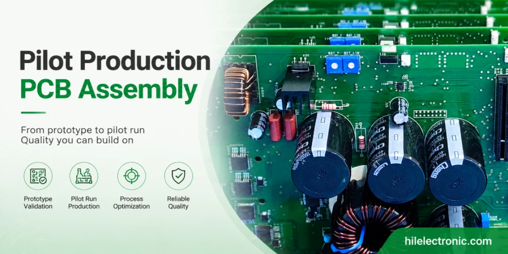
Mostre de inginerie should demonstrate that the approved construction can be fabricated and meet the agreed bare-board specifications. If the hardware will later be assembled, first articles can also provide early feedback on connector fit, BGA solderability and warpage exposure, but assembly yield is a separate result.
Productie pilot should preserve the physical stackup and process conditions while verifying panel utilization, test coverage, lot identification and handling of exceptions. A change from prototype flying-probe testing to volume fixture testing may be reasonable, but both must meet the required electrical acceptance; the proposed change should be documented.
Fabricație repetată needs a controlled laminate, process revision, customer-specific acceptance records and a defined material-change notification route. Changes to copper weights, via fill, surface finish or dielectric cannot silently be treated as routine purchasing substitutions. Where the finished card has firmware or BOM variants, coordinate the bare-board release with Highleap’s PCBA team rather than approving only a bare PCB part number.
When is a second prototype needed before pilot production?
An additional build or verification can be justified by a new substrate grade, revised via construction, altered impedance geometry, significant connector fit change or modified acceptance class. The engineering owner should decide the scope according to risk. A cosmetic silkscreen change need not trigger the same qualification as replacing a controlled-impedance dielectric stack.
When can engineering samples become a pilot release?
A prototype that meets its acceptance criteria can support a pilot build only when the proposed manufacturing route is stable. Highleap recommends preserving the approved stackup revision, laminate identity, via drawings, panel arrangement, critical fabrication notes and agreed inspection plan. The pilot order can then confirm repeatability at the intended quantity and identify any material or tooling differences before a larger production release.
If the product will be populated, assembly data should be part of the NPI package at this stage. Board panel rails, solder-mask details, surface finish, SMT pad flatness and component thermal constraints can affect whether the PCB is suitable for repeated assembly. A first board that passes electrical continuity can still create BGA yield or mechanical fit problems unless these interfaces were included in the review.
Gama de 14-layer PCB manufacturing and supplier scope covers the bare-board service, while 14-layer SMT and turnkey assembly extends the release process to components, programming and board-level functionality.
14 Layer PCB Production Transfer and Traceability
Production traceability should identify the customer part and revision, the material/stackup build, relevant fabrication lot and the required test results. Engineering deviations need recorded disposition and customer authorization. Changes to the dielectric grade, hole geometry, pad finish, copper profile or inspection plan may require additional evaluation before the next delivery.
A change in factory or specialist process route also deserves formal assessment. The assembly line should receive the correct board revision and any instructions affecting connector holes, panel break-off, cleaning or coating. Highleap can coordinate manufacturing documentation across these stages, while the applicable qualification plan remains the one defined for the product program.
What should be reviewed before increasing the order quantity?
Confirm the same approved materials and construction; acceptance evidence from the prototype or pilot lot; assembly compatibility; the component and fixture schedule if PCBA is included; and whether repeat manufacturing will use the same panel layout and testing route. Request a written list of deviations and the date of manufacturing release rather than depending on an earlier sample ship date.
Which transfer documents preserve supplier and lot traceability?
For a transfer from another manufacturer, provide the current approved Gerber/ODB++ files, fabrication stack, drill span drawing, impedance schedule, last accepted engineering questions, relevant coupon results, yield or field failure observations and packing configuration. If no manufacturing data are available beyond the Gerber set, note that the new factory may need to re-create and re-approve the physical cross-section.
For overseas OEM delivery, agree the shipping unit (individual PCB or panel), protective packing, requested certificates, lot marking, Incoterms and destination. If the equipment is safety- or reliability-critical, require the applicable documents from the actual nominated factory site, not only a brochure. Highleap’s China-based fabrication/EMS service can coordinate related tasks, but custom qualification steps should remain explicit purchase-order deliverables.
What is a reasonable basis for selecting a 14-layer prototype supplier?
Look for a documented proposed build, candid manufacturability exceptions, a test method for the highest-risk features and a schedule tied to actual material and process availability. Public capabilities can establish that Highleap is worth evaluating; a repeatable first-article record and agreed change-control process establish a much stronger basis for placing the next order.
Request a 14 Layer PCB Prototype Manufacturing Quote
Provide all copper/drill files, layer sequence, material and stackup data, final thickness, impedance and hole requirements, surface finish, sample and annual quantities, test/inspection scope and requested destination. Highlight any critical first-article measurements or reliability evidence in the drawing. Highleap can assess the manufacturing route, confirm technical questions and quote the relevant production schedule and inspection deliverables.
Share the NPI files, sample quantity, approved materials, first-article requirements and requested ship date.
Attach the engineering files and specify prototype quantity, future production forecast and which reports are needed for engineering acceptance.

Posturi recomandate
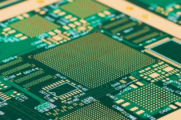
Producător de PCB HDI cu 14 straturi în China pentru plăci Microvia personalizate
HIGHLEAP ELECTRONICS / MICROVIA / SECVENȚIALĂ...
Producător de PCB cu 14 de straturi în China
PCB MULTISTRAT RIGID PERSONALIZAT Highleap Electronics...
Asamblare PCB cu 14 straturi și fabricare PCB într-o singură operațiune
FABRICAȚIE PCB + PCBA Highleap Electronics oferă 14...
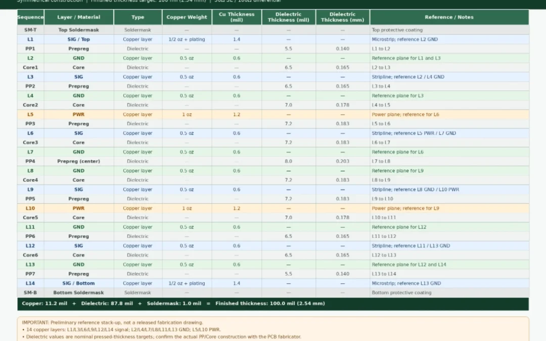
Suprapunere PCB cu 14 straturi pentru fabricație de mare viteză și multistrat
RECENZIE INGINERIE ȘI STACKUP Un PCB stackup cu 14 straturi este...
Cum să obțineți o ofertă pentru PCB-uri
Hai să executăm o analiză DFM/DFA pentru tine și să te contactăm cu un raport. Poți încărca fișierele în siguranță prin intermediul site-ului nostru web. Avem nevoie de următoarele informații pentru a-ți oferi o ofertă de preț:
-
- Specificații Gerber, ODB++ sau .pcb.
- Lista BOM dacă aveți nevoie de asamblare
- Cantitate
- Timp de întoarcere
Pe lângă fabricarea de PCB-uri, oferim o gamă completă de servicii electronice, inclusiv proiectare PCB, PCBA și soluții la cheie. Indiferent dacă aveți nevoie de ajutor cu prototiparea, verificarea designului, aprovizionarea cu componente sau producția de masă, vă oferim asistență completă pentru a asigura succesul proiectului dumneavoastră.
Pentru servicii PCBA, vă rugăm să furnizați lista de materiale (BOM) și orice instrucțiuni specifice de asamblare. De asemenea, oferim analize DFM/DFA pentru a optimiza proiectele dumneavoastră în ceea ce privește fabricabilitatea și asamblarea, asigurând un proces de producție fără probleme.