
12 Layer PCB Manufacturing FAQ: From Stackup to Assembled PCBA
Highleap Electronics provides custom 12 layer PCB fabrication and coordinated PCB assembly for OEM electronics. We review controlled-impedance stackups, HDI options, BGA fan-out, materials, inspection and volume manufacturing as one build-to-print project.
Use the sections below to check stackup feasibility, define inspection and assembly requirements, and prepare a complete manufacturing quotation package.

12 Layer PCB Manufacturer for OEM Electronics
Highleap Electronics provides build-to-print 12 layer PCB fabrication and coordinated PCB assembly for OEM and ODM hardware. A twelve-layer construction is appropriate when dense component escape routing, power distribution and high-speed reference planes must share one controlled stackup. Highleap can review standard plated-through-hole designs and advanced constructions that add selected blind or buried vias, controlled impedance, fine-pitch BGA footprints or special finishes. For the core production service and manufacturing options, see our 12 layer PCB fabrication service.
What products are suitable for a custom 12 layer PCB?
Products with significant signal-routing density, multiple voltage domains, high-speed interfaces or large BGA packages are strong candidates. The layer count should come from the routing and reference-plane requirements—not from a marketing category. We review board size, layer map, materials, components, required tests and expected order quantities before confirming the build route. For common applications and layer-count alternatives, see our 12 layer PCB application and selection guide.
Can Highleap manufacture both bare 12 layer PCBs and populated boards?
Yes. Highleap can coordinate the bare-board fabrication and the approved SMT/through-hole assembly scope, including sourcing and functional testing where separately agreed. The PCB artwork, stackup, bill of materials and assembly drawing are controlled as related revisions. Having one project owner helps resolve issues such as pad finish, BGA escape, press-fit tolerances and panelization before parts reach the assembly line.
Custom 12 Layer PCB Stackup, Layer Allocation and Thickness
We help OEM teams translate a 12-layer circuit design into a buildable stackup with defined copper weights, dielectric spacing and impedance requirements. The stackup must satisfy the electrical design and the press, drilling and assembly constraints at the same time. Five double-sided cores with outer foils is one possible build—not a universal construction for every twelve-layer board. Other core/foil arrangements and sequential-lamination configurations are used when the via architecture demands them.
What is a practical 12 layer PCB stackup?
An effective stackup assigns continuous reference planes next to critical signal layers and provides usable power distribution without excessive dielectric imbalance. The illustrated six-signal/six-plane example is only one allocation; a board with different BGA fan-out and power needs may use a different split. We review the layer sequence, copper thickness, final dielectric construction and manufacturability with the customer, using the multilayer PCB stackup design guidance as a starting point. The final proposal is approved against the OEM impedance table and mechanical requirements.
Is 1.6 mm the standard thickness for every 12 layer PCB?
No. A 1.6 mm finished thickness may be feasible in some twelve-layer builds, but fitting twelve copper layers and their dielectric separations into that envelope can make impedance traces, via aspect ratios and material availability restrictive. 2.0 mm, 2.4 mm or another specified thickness may be more appropriate. We quote against the actual mechanical envelope, mating connector requirements and drilled-hole sizes rather than treating one thickness as mandatory.
When is a 12 layer PCB better than 10 or 16 layers?
Twelve layers can be a good balance when ten layers cannot accommodate the routing plus solid reference planes, but sixteen layers would add unneeded layers and cost. This is a design trade-off, not a guaranteed price ratio: fine drill sizes, materials, HDI and panel yield can outweigh the difference in layer count. Review the most constrained interface and the number of genuinely needed reference planes before changing the PCB stackup.
Controlled Impedance and High-Speed Multilayer PCB
Highleap reviews 12 layer high-speed PCB builds for controlled-impedance single-ended and differential traces. Common applications include Ethernet, memory, SERDES, high-speed connectors and high-density processor modules. Impedance control is linked to dielectric thickness, actual copper cross-section, reference planes, solder mask loading and material properties; the number of layers does not independently determine a channel’s electrical performance.
How do I specify 50 Ω single-ended and 100 Ω differential traces?
Supply an impedance matrix listing layer, nominal target, allowable tolerance, trace type, reference planes and any fixed width/spacing constraints. The factory can then propose dielectric and finished-copper conditions and identify traces needing width adjustments for fabrication. Unless agreed otherwise, do not assume that every 12 layer design receives the same impedance tolerance. Our controlled-impedance PCB manufacturing process explains the design and coupon handoff.
Does TDR impedance testing prove that a multi-gigabit PCB channel works?
No. TDR can check the impedance of properly designed coupon structures, while high-speed channel insertion loss, return loss and crosstalk require the relevant S-parameter or system-level measurement plan. The laminate loss tangent, copper surface profile, route length, connectors and via discontinuities all matter. Highleap can discuss board-level acceptance requirements; specialized loss or link tests should appear explicitly in the quote. Our high-speed digital PCB manufacturing service addresses these material and channel considerations.
When should I select low-loss material rather than ordinary FR-4?
When a loss budget, frequency, trace length or temperature requirement shows that the selected FR-4 construction cannot meet the electrical margin. High-Tg FR-4 is not automatically a low-loss material: Tg relates to thermal transition behavior, while Dk/Df and copper roughness affect signal transmission. A hybrid low-loss/FR-4 stackup may work if material compatibility, bonding and tolerances are approved. Choose from actual material specifications and an engineering review, not the terms “high speed” or “12 layers” alone.
HDI 12-Layer PCB, Fine-Pitch BGA and Backdrilled Vias
A 12 layer PCB can be built with conventional plated through-holes or with advanced interconnect features when component pitch and board area require them. Highleap reviews blind and buried vias, microvias, resin-filled via-in-pad and backdrilling as distinct manufacturing requirements. Each must be identified by actual layer span, hole construction and intended assembly or high-speed function.
| خيار البناء | When OEMs request it | Key manufacturing review |
|---|---|---|
| Through-hole 12 layer PCB | Board has room for mechanical vias and routing | Finished thickness, mechanical drill, copper plating and annular ring |
| 12 layer HDI / blind-buried vias | Fine-pitch BGA escape or limited board area | Via span, microvia structure, registration, reliability and lamination sequence |
| Via-in-pad plated over (VIPPO) | Pads cannot escape without a via directly in the land | Filling, planarization, cap plating, X-ray and solderability |
| Backdrilled 12 layer PCB | Unused plated-through-hole stubs compromise a high-speed channel | Stub target, drilling side, depth control and layer clearance |
Does every 12 layer PCB need HDI or blind and buried vias?
No. Standard mechanical vias often meet the routing requirements of twelve-layer industrial and communications boards. HDI is justified when routing density, BGA escape or board size makes the conventional solution impractical. A buried via also does not automatically mean a particular microvia-based HDI build. Send a layer-span drill table and pad geometry so we can select the appropriate HDI PCB fabrication option rather than adding advanced processes by default.
When should a 12 layer BGA PCB use via-in-pad plated over?
Use via-in-pad when the BGA pitch or routing pattern leaves too little room for an external dog-bone escape. If the via is in a solderable land, the specified fill, planarization and plated cap must be suitable for the package and assembly process; ordinary tenting is not equivalent. Our filled and plated via-in-pad PCB construction is relevant to dense processor, memory and communication packages. We review the actual padstack and X-ray acceptance requirements before confirmation.
Will backdrilling improve every high-speed PCB?
Only when unwanted via stub length is materially affecting the channel. Backdrilling removes an unused part of a plated hole without cutting required layer connections; its usefulness depends on data rate, routing, stackup and connector geometry. The remaining stub limit, clearance to inner copper and inspection method must be specified. See our PCB backdrilling and stub-removal service for applications where it can reduce reflections.
12 Layer PCB Materials, Copper Weight and Surface Finish
Highleap evaluates standard FR-4, higher-performance laminate options and special copper/finish requirements for 12 layer board designs. Materials are chosen for the released electrical, thermal and processing requirements—not simply because the PCB has twelve layers. Heavier copper, special finishes or a hybrid laminate can all be appropriate, but each affects trace geometry, resin flow, board flatness and assembly.
Can a 12 layer PCB use heavy copper and fine-pitch BGA pads?
Potentially, but this is a difficult mixed requirement. Thick copper needs additional etch clearance and dielectric filling, while fine-pitch pads demand tight imaging and solder-mask control. The combination may require different copper weights by layer or a revised stackup. Highleap can review a heavy copper PCB manufacturing project against the actual copper map; no specific current rating can be inferred from copper ounces alone.
Which surface finish is suitable for a 12 layer PCB with BGA and gold fingers?
The BGA solder lands and the edge-connector contacts perform different jobs. Flat solderable finishes such as ENIG or qualified alternatives may suit fine-pitch SMT, while repeated mating often calls for appropriately specified electrolytic hard gold fingers with the correct bevel and thickness. A combined-finish design needs a clear area map and suitable manufacturing routing. Review the gold finger PCB finishing requirements before the connector design is frozen.
Is a high-Tg laminate always necessary for lead-free assembly?
No universal Tg number should be prescribed from layer count alone. Laminate selection depends on the full reflow profile, number of cycles, Z-axis expansion, via reliability and the applicable material datasheet. Highleap can review high-Tg PCB laminate choices alongside the customer’s soldering sequence, rather than substituting a material without approval.

Multilayer PCB Fabrication, Electrical Test and Quality Control
For a 12 layer multilayer PCB, quality control must cover the internal copper patterns, layer registration, through-hole plating, finished geometry and any separately specified impedance tests. Highleap supports manufacturing reviews and project-defined inspection plans for prototype and production quantities. Acceptance requirements need to be agreed before fabrication—not inferred from a generic statement that a board is “tested.”
| Manufacturing / verification stage | ما الذي يتم فحصه؟ | What the evidence does not prove |
|---|---|---|
| Inner-layer AOI and registration | Copper opens/shorts, alignment and registration before final lamination | Completed-board electrical function |
| Drilling and plating checks | Hole size, annular ring, plated-hole condition and relevant coupon cross-sections | Every via under all possible thermal cycles |
| اختبار كهربائي للوحة العارية | Continuity and isolation against the approved netlist | Impedance, signal loss or programmed functionality |
| Impedance coupons / TDR | Specified single-ended or differential impedance for representative structures | System-level data rate, EMC or connector channel performance |
| Finished-board visual / dimensional | Solder mask, finish, outline, thickness, bow/twist and workmanship | Populated-board assembly yield or end-device compliance |
How are hidden inner layers inspected before lamination?
Copper artwork is inspected before the layers are permanently pressed together; registration and copper integrity are key early checkpoints. The completed board also needs appropriate hole and plated-interconnect verification, which may include microsections or additional tests by agreed sampling plan. Highleap’s PCB fabrication and engineering review service covers the manufacturing route, but exact report content should be written into the purchase specification.
Does 100% electrical testing mean the board is fully qualified?
No. A bare-board netlist test primarily establishes continuity and isolation. It does not establish impedance, high-frequency loss, BGA solder integrity or complete operation of a populated product. Those are separate controls, with their own acceptance requirements. See bare-board electrical testing options and specify any panel-coupon, cross-section or functional evidence the program needs.
Which IPC acceptance class should be specified for a 12 layer PCB?
The OEM should identify the applicable rigid-board fabrication specification and product class in the released drawing; an agreed IPC-6012 requirement is different from the inspection of assembled solder joints under IPC-A-610. Higher-reliability products may need Class 3 or additional project-specific testing, but an industry label such as “medical” or “automotive” does not automatically define the entire inspection package. The manufacturing facility and certification scope also need separate confirmation.
Turnkey 12 Layer PCB Assembly and BGA Production
Highleap can coordinate 12 layer PCB fabrication with SMT, through-hole assembly, approved component sourcing and agreed PCB-level inspection or functional testing. For an OEM ordering populated twelve-layer boards, manufacturability must be reviewed across both stages. A stackup can be fabricable yet difficult to populate if the board warps, large BGAs lack reliable solder lands or test access is absent.

Can Highleap assemble fine-pitch BGA packages on a 12 layer PCB?
Yes, subject to the actual pitch, package, board outline, stencil and fixture plan being accepted for the assigned assembly line. Hidden BGA solder joints need an appropriate inspection plan; BGA PCB assembly and inspection is relevant for dense processor modules and communication boards. A bare-board electrical test does not validate those joints after reflow, so X-ray criteria and any programmed test must be listed separately.
Who controls BOM sourcing and approved component substitutions?
The OEM controls design intent and approves alternatives that change the approved BOM. Highleap can coordinate electronic component procurement and BOM review and flag end-of-life or allocation risks, but form/fit/function similarity alone is not approval. Quote the procurement model clearly: consigned parts, partial turnkey or full turnkey. The BOM revision, DNP options and traceability level are part of the manufacturing package.
What does turnkey 12 layer PCBA include beyond SMT placement?
The scope can include bare PCB procurement, BOM sourcing, SMT and through-hole soldering, programming, selected X-ray/AOI, functional test and packing—but only the agreed items are part of the quote. Our turnkey PCB assembly and production service explains the sourcing and handoff model. For a complete board set or enclosure build, include harnesses, firmware, fixtures and final functional-test responsibilities in the order.
12 Layer PCB Prototype Pricing and Production Lead Time
A twelve-layer PCB quote is driven by construction details, not layer count alone. Two drawings with the same width, height and twelve layers can differ markedly in price if one requires standard through vias while the other needs multi-stage HDI, premium low-loss materials, backdrilling, filled pads or extra inspection. Costs also depend on panel yield, finished thickness, material availability and quantity.
How much does a custom 12 layer PCB cost?
There is no reliable single unit price without the drawing and the order quantity. A small prototype with fine drills and a controlled-impedance coupon can cost more per board than a larger production lot, while low-loss or HDI construction can change the price disproportionately. To compare offers, check whether laminate part numbers, stackup approval, electrical testing, impedance documentation, tooling, shipping and any PCBA work are actually included.
How long does 12 layer PCB manufacturing take?
Lead time should be quoted for the released design rather than promised as a universal day count. A standard-material through-hole construction may have a different schedule from a board requiring sequential lamination, special laminate sourcing, large copper weights or extra validation. Ask for the engineering-release date, manufacturing lead time, assembly lead time and shipment date separately. Highleap’s PCB manufacturing lead-time guidance explains the principal variables.
Should I order 12 layer PCB prototypes before a volume release?
For a new stackup, new BGA package or changed material, prototypes and a controlled first build help validate mechanical fit, impedance assumptions and the intended assembly route. Pilot quantities can establish inspection methods, yield risks and configuration records before higher-volume purchase orders. Our PCB prototype and NPI manufacturing services can be scoped with the downstream production quantity in mind, so the sample route is not accidentally different from the planned manufacturing route.
Request a Custom 12 Layer PCB Quote: Gerber and RFQ Checklist
To obtain a useful 12 layer PCB manufacturing quote, send the board files together with the decisions that influence stackup, drilling, impedance and assembly. If some parameters are still open, identify them explicitly so Highleap can quote a proposed construction for approval rather than silently substituting materials or drilling structures.
What files are needed for a 12 layer PCB fabrication and assembly quote?
For bare boards, send the complete copper/drill data, board outline, target thickness, layer map, material preference, copper weights, impedance requirements, surface finish and acceptance class. For assembled boards, add the BOM, centroid file, assembly drawing, approved alternatives, firmware and functional-test requirements as relevant. Our مراجعة تصميم لوحات الدوائر المطبوعة لأغراض التصنيع can identify incomplete or conflicting data before a build is committed.
Can Highleap review an existing 12 layer PCB design before manufacturing?
Yes. Submit your released or preliminary drawing and identify any fixed constraints such as finished thickness, connector interfaces, high-speed channel loss or hole dimensions. We can review feasibility, flag manufacturability risks and propose items that need OEM approval. The customer remains responsible for design function and final change authorization. We can then propose an approved manufacturing route and clarify the test and quotation scope before production.

مقالات ذات صلة
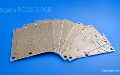
تصنيع لوحات الدوائر المطبوعة RO3203
دليل عملي لتصنيع لوحات الدوائر المطبوعة (PCB) من نوع روجرز RO3203 للدوائر اللاسلكية المدمجة، يغطي التحكم في المواد، وقرارات تصميم طبقات الترددات اللاسلكية، وفحوصات التصنيع، والتفتيش.
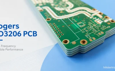
تصنيع لوحات الدوائر المطبوعة RO3206
دليل عملي لتصنيع لوحات الدوائر المطبوعة (PCB) من نوع روجرز RO3206 للمنتجات اللاسلكية المصغرة، يغطي التحكم في المواد، وقرارات تصميم طبقات الترددات اللاسلكية، وفحوصات التصنيع، والتفتيش.
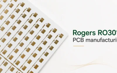
تصنيع لوحات الدوائر المطبوعة RO3010
دليل عملي لتصنيع لوحات الدوائر المطبوعة (PCB) من نوع روجرز RO3010 لدوائر الميكروويف المصغرة DK 10.2، يغطي التحكم في المواد، وقرارات تصميم طبقات الترددات الراديوية، والتصنيع.