
Smart Ring PCB | Kompakt fleksibelt kredsløb til wearables
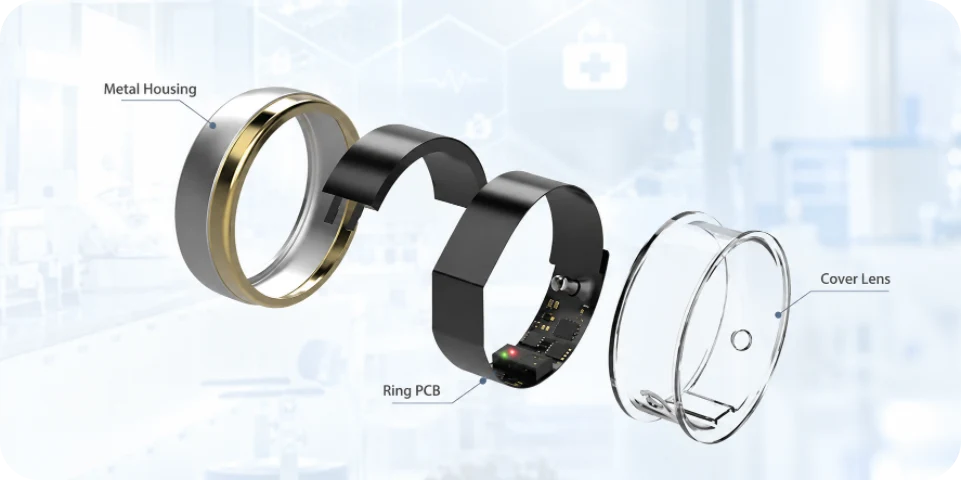
A smart ring PCB has to fit sensing, BLE, power and charging into a curved enclosure with almost no spare space. For an OEM or product team, the manufacturing question is not simply how small the PCB can be, but whether the released design can be fabricated, assembled, inspected and repeated at the required yield.
Flex or rigid-flex construction, HDI, microvias and fine-pitch packages can solve real space constraints, but each one adds process and cost implications. The right combination should be chosen from the mechanical envelope, component pitch, bend zones and production volume rather than specified by default.
Highleap Electronics supports customer-designed wearable electronics through elektroniske fremstillingstjenester, including PCB fabrication, flex and rigid-flex manufacturing, component sourcing, fine-pitch SMT assembly, inspection, programming and customer-defined functional test. We can support prototype, pilot and repeat production while the customer retains responsibility for antenna tuning, biometric algorithms, enclosure design and final product validation.
Smart Ring PCB Architecture Is Driven by the Mechanical Envelope
| Miljø | Produktionsrisiko | Fokus på produktion |
|---|---|---|
| Fleksibel / stiv-fleksibel | Bend stress, thin construction, forming variation | Defined bend zones, stiffeners, forming and handling controls |
| HDI / fine-pitch packages | Via fill, solderability, inspection access | Stack-up review, via-in-pad control, fixture and inspection planning |
| RF / antenna | Detuning from body, battery and enclosure | Preserve keep-outs, matching BOM and released geometry |
| Sensors / battery | Placement sensitivity, current peaks and limited internal volume | Placement accuracy, power-path checks and customer-defined test |
A useful smart-ring RFQ starts with the mechanical cross-section, released PCB construction and the target build stage. With those inputs, a manufacturer can judge whether conventional multilayer, flex, rigid-flex or HDI is actually needed and where the main yield risks will be. Highleap can review the manufacturing package from that perspective before prototype or pilot assembly.
Flex and Rigid-Flex Decisions That Affect Assembly
Flex is valuable when the circuit must follow the ring circumference, while rigid-flex can create stable component islands without using miniature board-to-board connectors. The manufacturing drawing should clearly identify bend zones, stiffeners, rigid-flex transitions and whether the flex is formed once during assembly or repeatedly flexed in use.
For procurement, the useful comparison is not bare-board price alone. A higher-cost rigid-flex design may still reduce total assembly cost if it removes connectors, lowers z-height and reduces manual interconnect work. Highleap can review the released stack-up and forming requirements together with the assembly process so the selected construction is practical to build repeatedly.
Use HDI Where Density Actually Requires It
WLCSP, BGA and small LGA packages can make microvias or via-in-pad necessary, especially when the ring diameter leaves little routing area. But HDI should solve a real escape or space problem, not be added as a default specification. If conventional drilling can meet the mechanical envelope and routing density, it can offer a simpler process and more sourcing flexibility.
When HDI is required, PCB fabrication and assembly should be reviewed together. Via fill and planarization, thin-board support, paste printing, reflow, inspection access and depanelization all affect the final PCBA yield. This is where early DFM review can prevent a dense design from becoming difficult to assemble consistently.
Preserve RF Geometry Through Manufacturing
Smart-ring BLE performance is strongly affected by the wearer, battery, enclosure and nearby metal. Manufacturing cannot replace final antenna validation, but it can protect the released RF design by preserving antenna keep-outs, ground geometry, matching components and component placement.
RF matching parts should also be tightly controlled in the BOM. A same-value substitute may have different high-frequency behavior, so alternates should follow the customer’s approved list or RF engineering approval. Production functional test can screen communication failures, missing parts and gross assembly defects, while final antenna performance remains a product-level validation task.
Once the design and test baseline are stable, Highleap can transfer the approved build into højvolumen PCB samling with controlled BOM revisions, repeatable inspection and customer-defined functional testing.
Highleap Electronics supports prototype, pilot and volume builds for customer-designed smart ring PCBAs, including flex or rigid-flex fabrication, HDI, component sourcing, fine-pitch SMT, inspection and functional test. Share the project information you already have and we can review the next manufacturing step with you.
PPG Sensor Placement and Optical Performance
For a smart ring, PPG performance depends on more than choosing the optical sensor. The PCB must hold the LED, photodetector and supporting components in the released geometry, while the final ring maintains the intended skin contact, optical barrier and window alignment. For manufacturing, the priority is repeatability: placement, cleanliness and mechanical reference points should remain consistent from prototype through production.
| Optical design item | Hvorfor det betyder noget | Fokus på produktion |
|---|---|---|
| LED / photodiode spacing | Controls the optical path through tissue | Placement accuracy and board/mechanical datum consistency |
| Optical barrier / window | Limits direct light leakage and ambient-light interference | Keep-outs, cleanliness, sensor height and enclosure tolerance |
| LED current / sensor orientation | Affects signal level, power, heat and optical direction | BOM control, polarity/orientation inspection and test mode |
The optical sensor may integrate the photodiode, analog front end and ADC, or use separate LEDs and receiver components. In either case, a board can pass digital communication and still fail in the finished ring if flux residue, adhesive, protective film or mechanical offset affects the optical path. PCBA inspection should therefore verify both electrical function and the released optical assembly requirements.
Keep PCB and mechanical datums aligned
Highleap Electronics can control placement and assembly against the released PCB data, but final biometric performance still depends on enclosure fit, skin contact and algorithm validation. If optical calibration is part of the product flow, the customer-defined method should be applied at the appropriate assembly stage rather than inferred from PCBA inspection alone.
Battery, Charging and Power Architecture for a Smart Ring
Battery capacity is limited in a smart ring, so both sleep current and short high-current events matter. BLE transmission, PPG LED pulses, sensor sampling and memory activity should be considered together when reviewing the power path. The PCB manufacturer can verify the released power design and defined current states, while firmware scheduling and final runtime remain product-level responsibilities.
Design for peak current, not only sleep current
The battery, PMIC and local decoupling must support radio and optical-current peaks without rail droop or resets. For production, customer-defined sleep-current and active-current limits can be useful screening tests for wrong parts, leakage, solder defects or configuration issues.
Charging method changes the manufacturing process
Contact charging requires controlled pad dimensions, finish, cleaning and handling because those surfaces may also be exposed to sealing and corrosion risks. Inductive charging removes exposed contacts but adds coil position, magnetic components and charging heat. In both cases, the production package should define the released charging geometry so assembly changes do not alter electrical or thermal behavior.
Charging can also warm a very small enclosure and influence nearby temperature sensing. Manufacturing can verify charge current, basic handshaking and customer-defined functional limits, while final battery safety, thermal limits and runtime validation remain part of the finished-product qualification plan.

Smart Ring PCBA: Fine-Pitch Assembly, Flex Handling and Inspection
A highly miniaturized smart ring may use 0201 or 01005 passives, WLCSP/BGA packages and small LGA sensors. When those packages are present in the released design, yield depends on more than placement capability. Panel stability, stencil release, support tooling, reflow behavior and inspection access all need to work as one assembly process.
Control the process around thin and flexible boards
Thin flex or rigid-flex panels may need dedicated support during paste printing, placement and reflow. Very small apertures require stable stencil release, while uneven thermal mass can increase soldering variation. Panel rails, copper balance and fixture design should therefore be reviewed before the first production lot rather than corrected after recurring defects appear.
Use the inspection method that matches the package
AOI is useful for visible polarity, missing parts and solder defects. X-ray may be appropriate for WLCSP/BGA or hidden pads, while optical sensor windows may need separate cleanliness inspection. No single inspection method proves RF or biometric performance, so production inspection should be combined with the customer-defined electrical and functional test scope.
Protect the flex and sensor surfaces during handling
Small flex assemblies can be damaged by creasing, contamination or uncontrolled bending. Work instructions should define grip areas, tray orientation and forming limits so operators do not use the antenna or optical-sensor region as a handling tab.
Smart Ring Prototype Manufacturing Challenges
A smart ring prototype should prove that the design can survive the real assembly process, not only that it works flat on a bench. Before moving to pilot or volume production, the build should answer the manufacturing questions most likely to create rework or yield loss.
- Can the flex be formed into the enclosure without stressing component pads or rigid-flex transitions?
- Does the battery preserve antenna keep-outs and the optical cavity after final assembly?
- Do BLE and PPG functions still meet the customer-defined acceptance criteria in the assembled ring?
- Can charging, programming and functional test be completed after the board is formed?
- Can the assembly be handled, depanelized and packed without damaging flex or optical surfaces?
Prototype-only debug pads or connectors should also have a clear production replacement plan. Highleap Electronics can use the early build to identify assembly, tooling, inspection and test issues before the design is transferred to pilot or repeat production. A customer does not need a perfect RFQ package to start the discussion; available Gerber/ODB++, BOM, flex drawings, target quantities and test requirements can be reviewed progressively.
From Smart Ring Prototype to Mass Production
Volume manufacturing shifts the focus from “can we build it?” to “can we build the same thing repeatedly?” The BOM needs approved alternates. Flex material and thickness need control. SMT fixtures, reflow and depanelization need repeatability. Programming and test must fit within cycle-time targets. These are the areas that determine yield and cost more than the marketing specification of the ring.
DFM og DFA
Before production release, review component-to-edge clearance, flex transition geometry, solder-mask web, via-in-pad, battery attachment, charging contacts, optical apertures and antenna keep-outs. DFA should also check whether operators can orient the formed flex correctly and whether the battery or enclosure can be installed without pressing on components.
Styklistetilgængelighed
Wearable sensors and miniature packages can have long lead times or limited alternates. Procurement risk should be identified before the enclosure is locked around one unique package. An alternate may require a different optical window, antenna match or footprint, so “second source” is often an engineering project rather than a purchasing substitution.
Functional test and yield
Production can check programming, sleep current, sensor communication, BLE link, charging and basic optical response. Test data should be tied to board revision and serial number when traceability is required. Yield targets should be measured separately for bare PCB, SMT, flex forming and final functional test so the team knows where cost is being lost.
Highleap Electronics can support the released PCB fabrication and PCBA stages. Final ring sealing, RF characterization, biometric algorithm validation and product certification should remain with the OEM or other specifically qualified partners unless separately contracted.
How to Choose a Smart Ring PCB and PCBA Manufacturer
A smart ring supplier needs more than ordinary small-board SMT. The manufacturing partner should understand how flex construction, HDI, tiny packages, antenna geometry and optical sensor placement interact. The most useful factory feedback happens before tooling and panelization are frozen, when the design can still absorb DFM changes without disturbing the enclosure.
- Flex and rigid-flex fabrication for the actual released stack-up.
- HDI/microvia/via-in-pad processing when the package escape requires it.
- Fine-pitch SMT and fixtures for thin or flexible assemblies.
- Controlled sourcing for BLE SoC, PPG sensor, IMU, PMIC and RF matching components.
- AOI/X-ray/optical inspection selected according to package and sensor risk.
- Programming, sleep-current checks, BLE and customer-defined functional test.
- Documented transfer from prototype panel/process to repeat production.
RFQ-pakke
- Gerber/ODB++, complete flex/rigid-flex fabrication drawing and stack-up.
- Microvia, via-in-pad, stiffener and final thickness requirements.
- BOM with approved alternates and do-not-substitute RF/optical components.
- Pick-and-place and assembly drawings with antenna and optical keep-outs.
- Mechanical datum or outline information needed for sensor/window alignment.
- Battery/charging interface information included in the PCBA scope.
- Programming files, serialization requirements and functional-test specification.
- Prototype quantity, pilot quantity and expected production forecast.
When these inputs are available, Highleap can review the actual manufacturing risks and provide a PCB/PCBA quotation. The goal is not to make every ring use the most advanced PCB technology; it is to use only the complexity necessary to meet the released mechanical, RF, optical and reliability requirements at a repeatable production yield.
Ofte stillede spørgsmål
Does every smart ring require a flex or rigid-flex PCB?
No. Flex and rigid-flex are attractive because they conform to a curved enclosure and can eliminate connectors, but some designs use miniature rigid boards or other interconnect structures. The mechanical architecture should decide.
Why is HDI common in smart ring PCB designs?
Very small board area and fine-pitch packages can make conventional through-via escape inefficient. Microvias and via-in-pad can improve routing density when those constraints justify the added fabrication complexity.
Can a smart ring PCB use 01005 components?
It may, if the mechanical density requires them and the assembly process supports reliable stencil printing, placement and inspection. Designers should not select ultra-small packages unless they provide a real size advantage.
Why is the BLE antenna difficult in a smart ring?
The antenna operates close to the finger, battery, ground copper and enclosure materials. Human-body loading and nearby metal can detune the antenna, so final tuning must be validated in the assembled ring.
How does PCB assembly affect PPG sensor performance?
Placement, optical cleanliness, LED/sensor orientation and board-to-enclosure alignment all matter. However, skin contact, optical barriers, windows and algorithms are also system-level factors.
What should be tested during smart ring prototype manufacturing?
Verify flex forming, battery fit, antenna performance, charging heat, sensor alignment, sleep/peak current, programming access and assembly yield—not only whether the MCU boots.
What files are needed for a smart ring PCB/PCBA quote?
Provide Gerber/ODB++, flex/rigid-flex drawings, stack-up and HDI requirements, BOM, placement/assembly drawings, antenna/optical keep-outs, programming/test files and build quantities.

anbefalet Indlæg

Top 8 hukommelseschipproducenter i verden
Hos Highleap Electronics, en førende PCB-produktion og...

QFP indkøbs-, monterings- og emballageløsninger
Hos Highleap Electronics er vi stolte af at være en...

PCB BOM-guide | Omkostningseffektiv sourcing og BOM PCB-styring
[pac_divi_table_of_contents title="På denne artikel"...

Rollen af PCB-design og -fremstilling i optimering af HDMI-modulatorydelse
[pac_divi_indholdsfortegnelse...
Sådan får du et tilbud på printkort
Lad os køre en DFM/DFA-analyse for dig og vende tilbage til dig med en rapport. Du kan uploade dine filer sikkert via vores hjemmeside. Vi har brug for følgende oplysninger for at kunne give dig et tilbud:
-
- Gerber, ODB++ eller .pcb, spec.
- Stykliste, hvis du ønsker montering
- Antal
- Vendetid
For PCBA-tjenester bedes du fremvise din BOM (Bill of Materials) og eventuelle specifikke monteringsinstruktioner. Vi tilbyder også DFM/DFA-analyse for at optimere dine designs med hensyn til fremstillingsevne og montering, hvilket sikrer en problemfri produktionsproces.