
HIGHLEAP ELECTRONICS / MICROVIAS / SEQUENTIAL BUILD-UP
14-lags HDI PCB-producent i Kina til brugerdefinerede Microvia-kort
Highleap Electronics provides custom 14 layer HDI PCB manufacturing in China for compact, high-density OEM electronics. Our multilayer PCB program covers engineered blind and buried via structures, laser microvias, copper-filled microvias and filled-and-capped via-in-pad requirements, fine-line routing and coordinated assembly when the design calls for populated boards. Highleap’s published HDI fabrication capabilities include 1+N+1, 2+N+2 and 3+N+3 construction families; the approved fourteen-layer build depends on the actual via spans, laminate system, registration and reliability requirements.
A 14-layer HDI design must be quoted as a complete interconnect structure. Copper-layer count alone does not confirm microvia depth, the number of sequential lamination cycles or available BGA breakout. For a conventional through-hole multilayer alternative, the 14 layer PCB manufacturing service covers the broader rigid-board scope. HDI production adds its own material, process and inspection decisions.
Send the via-span drawing, build-up stackup, Gerber or ODB++ files and target quantity. Add the BOM if assembly is required.
14-Layer HDI PCB Capabilities and Applications

Highleap can coordinate fabrication from released Gerber/ODB++ files, netlist and drill data, a construction drawing and the requested quality plan. Its public tabel med stive printkortkapaciteter lists a wider multilayer, laser-drilling and fine-line process envelope. Those are individual capability limits, not approval to combine maximum thickness, minimum microvia, narrowest line and highest copper weight on one 14-layer design. The factory engineering review establishes which combination can be released.
Typical manufacturing deliverables include the approved physical stackup, layer-span drill definitions, selected laminate and copper specifications, a manufacturing panel plan, bare-board electrical test and any ordered impedance or microsection records. The scope can be prototype, low-volume or repeat production; the component BOM and assembly acceptance are added when PCBA is included. A single engineering contact can coordinate these steps without implying every specialist process happens in the same physical production room.
Can a Chinese supplier manufacture both the HDI board and a tested PCBA?
Highleap offers PCB fabrication and electronic assembly services. A turnkey order can include the specified boards, approved component sourcing, SMT/THT placement, firmware loading and board-level functional testing; these are separately defined quotation deliverables. Laser-via registration, via-fill quality and PCB solderability remain bare-board responsibilities, while hidden BGA solder joints and populated-board behavior require assembly inspection and tests. The related Nøglefærdigt PCB-monteringsprogram defines how the scope can be coordinated.
14 Layer HDI Boards for FPGA, Networking and Industrial Computing
Highleap can evaluate high-density FPGA and SoC carrier boards, industrial computing modules, image-processing controllers, network-switch interface cards, compact telecom hardware and data-acquisition products. The fabrication requirement changes with the board: dense processor modules prioritize BGA fan-out and power-plane continuity; a network card may prioritize low-loss channels and backdrilled transitions; an industrial control board may prioritize isolation and connector robustness.
These product categories are manufacturing application types, not claims of unnamed customers or validated end-system certifications. For networking channels where copper roughness, material loss and connector transitions dominate performance, our high-speed PCB manufacturing guidance addresses those separate loss and channel concerns, alongside the wider high-speed PCB fabrication service.
What separates an HDI manufacturer from a conventional multilayer PCB factory?
A fourteen-layer rigid board with ordinary plated through-holes can be fabricated without laser build-up layers. HDI adds a sequence of material preparation, fine-feature imaging, laser drilling, desmear, copper deposition, filling and re-lamination where the approved design requires it. The vendor must explain which operations are included and which interconnects they qualify, rather than relying on the layer count as a capability claim. For a staggered microvia build, the inspection strategy will differ from a multi-high stacked-via column over a buried core connection.
When comparing quotes, request the proposed build-up sequence, the minimum registration margin used for the actual microvia pads, any permitted via-fill void criteria and an indication of which structures require cross-section coupons. Production transfer should preserve those features and the laminate source—not just a Gerber revision number.
HDI Stackups, Blind/Buried Vias and Stacked Microvias
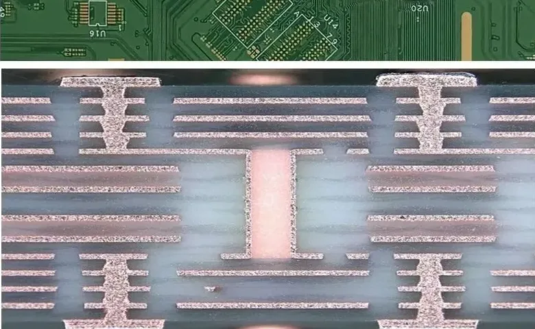
A symmetric 14-layer HDI notation describes the central copper-layer core and the build-up layers added on each face. For example, 2 + 10 + 2 denotes two build-up copper layers on each side of a ten-layer central structure; it does not, by itself, define the exact dielectric thickness, all via connections or the number of finished laser-drill operations. The final engineering drawing must trace every blind, buried and plated through connection through the approved press sequence.
| 14-layer build-up | Structure represented | Primary DFM checks |
|---|---|---|
| 1 + 12 + 1 | One build-up copper layer per face of 12-layer central core. | Laser via span, core PTH, pressed dielectric and BGA escape. |
| 2 + 10 + 2 | Two build-up layers per face of 10-layer central structure. | Stacked/staggered vias, filling and lamination registration. |
| 3 + 8 + 3 | Three build-up layers per face of 8-layer core. | Complex via stack, thermal reliability, material availability and yield. |
The notation counts copper layers; the approved drill-span table and cross-section define the actual interconnect.
The goal is to use the simplest build-up sequence that permits the approved fan-out, return paths and mechanical construction. A 3+8+3 build-up does not necessarily use three vertically stacked microvias; if a three-high stack is proposed, its reliability and acceptance testing need separate approval. An additional HDI step increases imaging, lamination, drilling, plating and registration work. Asymmetric designs may be appropriate if dense devices are on only one side, but the resulting copper balance and flatness require specific review. Highleap’s lamination and multilayer process information provides the surrounding fabrication context.
Is 3+8+3 automatically better than 2+10+2 for a 0.4 mm BGA?
No. BGA pitch matters, but so do the package ball map, the available escape channels, the padstack, routing-layer assignment and via structure. A 2+10+2 arrangement can be adequate for some fine-pitch devices, while others need a different build-up or a revised processor breakout. Send the BGA land-pattern drawing and the full drill-span map rather than ordering a more expensive lamination sequence by name.
Blind, Buried, Stacked and Staggered Microvia Fabrication
Laser-drilled blind microvias typically connect adjacent copper layers; longer interconnect paths use separately specified via structures across the approved build-up sequence. Buried connections are completed within the laminated interior before the outer build. Stacked microvias create vertically aligned transitions between successive layers, whereas staggered structures use an offset transition. These alternatives differ in copper plating, via fill, mechanical stress distribution and qualification. The via map must identify each layer pair and whether the interconnect is copper filled, resin filled or open by design.
Copper-filled microvias and plated-over lands are not interchangeable with ordinary solder-mask-tented vias. The specified fill, cap thickness, surface flatness and void acceptance should be set before production. Where reliability is critical, request cross-sections together with a performance-based test-coupon method appropriate to the assembly thermal profile; do not treat a passing room-temperature continuity test as proof of thermal-cycle endurance.
Can stacked microvias be placed directly over a buried via?
Such structures exist, but they create a demanding interconnect and should be separately reviewed for manufacturing yield and thermal reliability. The drawings must identify the buried via fill/cap, the stacked laser-via spans, annular geometry and the allowed registration error. A supplier should confirm the approved process and any required structural verification before accepting a stack height as routine.
HDI Materials, BGA Escape and Via-in-Pad
Highleap can review standard and high-Tg FR-4, specified low-loss digital laminates, appropriate RCC/build-up materials and mixed-dielectric constructions. Material selection must satisfy the sequential lamination schedule, laser-drilling behavior, copper adhesion, via filling and thermal stress, as well as any insertion-loss or impedance requirements. A nominal dielectric constant alone is not sufficient evidence that a substitute laminate will work in a particular HDI stack.
| Materialefamilie | Relevansen af produktionen | Procurement condition |
|---|---|---|
| Standard / High-Tg FR-4 | Common multilayer base, subject to compatibility with the HDI build-up cycle. | Confirm Tg, CTE, copper foil, press system and stock format. |
| Low-loss digital laminate | Where high-speed insertion-loss targets require a specific Dk/Df system. | Specify exact grade, frequency-dependent datasheet and allowed alternatives. |
| RCC / build-up dielectric | Can support defined laser microvia structures on selected HDI processes. | Validate dielectric thickness, drilling, adhesion, via copper and thermal stress. |
| Mixed-material laminate | Possible for hybrid RF/digital requirements after qualification. | Do not substitute by nominal Dk alone; evaluate resin and lamination compatibility. |
MEGTRON, Isola, ITEQ, Rogers and Shengyi are material inquiry families, not a claim that every grade is stocked or compatible.
Brand-specific RFQs may name Panasonic MEGTRON 6 or 7, Shengyi, Isola, ITEQ or Rogers product families. These names should be supplied with the exact grade and approved material datasheet, because each brand contains products with very different chemistry and intended use. Highleap can evaluate availability and process compatibility through its high-layer-count laminate sourcing guidance. This is not a claim that every material is held in stock or that every RF-grade material can tolerate the same HDI press sequence.
Can Highleap source customer-specified low-loss or halogen-free laminate?
A material-controlled RFQ can include the approved manufacturer, grade, core/prepreg combination and substitutions policy. Availability, stock format, lead time and HDI process compatibility must be confirmed for the project. If the exact grade is unavailable, an alternative should only be proposed with its electrical, thermal and lamination implications documented for customer approval. “Equivalent Dk” is not sufficient approval for an unreviewed material change.
Fine-Line HDI Routing, BGA Escape and Via-in-Pad
Fine-pitch BGA escape relies on the combination of trace/space, solder-mask definition, microvia pad size, copper thickness and available internal routing layers. Highleap’s published rigid-board limits show fine-line process capability, but the smallest advertised geometry should not be assumed to coexist with every thick copper, large-panel or mixed-material design. CAM review checks the actual artwork and panel registration.
A 14-layer FPGA or SoC carrier may need plated-over via-in-pad beneath selected BGA pads so that routing can change layers without sacrificing pad area. The via-in-pad fabrication service provides the process background. For a true solderable pad, specify the fill method, planarization and cap plating rather than using “plugged via” as an ambiguous callout.
What pad and trace dimensions are required for a 14-layer HDI quote?
Include the BGA pitch and manufacturer footprint, copper-pad diameter, solder-mask openings, minimum line and space by layer, drilled and finished microvia diameters, minimum annular ring and the copper weight after plating. Highleap can then review whether the smallest features are compatible with the proposed HDI sequence, material and assembly route. Numerical process minima are confirmed against that exact build.
Microvia Reliability, Quality Control and Supplier Qualification
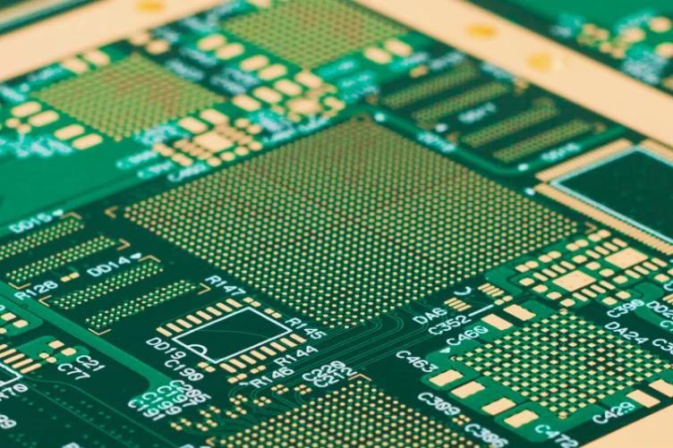
A 14-layer HDI acceptance plan can specify inner-layer AOI, registration checks, laser-drill quality, plating and via-fill cross-sections, finished-pad inspection, continuity/isolation testing, and impedance coupon verification where applicable. Test reports should identify the coupon or lot, acceptance criteria, relevant sampling and the agreed standard. Product environmental qualification, solder-joint inspection and functional testing are separate from these bare-board checks.
The requested IPC-6012 rigid-board performance class and IPC-A-600 acceptability criteria should be identified in the fabrication documentation. Specialized HDI requirements and reliability screening should be attached to the customer order; a generic phrase such as “100% inspected” does not establish destructive-test sampling or microvia thermal-cycle compliance.
How should stacked microvia reliability be confirmed?
Specify the microvia cross-section features to examine, the coupon or representative sample, any required thermal-stress/thermal-cycle profile and the accept/reject conditions. A microsection can document geometry and visible defects at the sampled location; it does not prove every hidden interconnect in every delivered board will survive every mission profile. A complete qualification plan belongs to the specific product and approved manufacturing route.
HDI Supplier Qualification and Documentation Control
High-density boards have several non-interchangeable acceptance criteria. A useful engineering response identifies the nominated substrate grade, core/build-up architecture, allowable microvia stacking, plating/fill plan, sample qualification and how a future material or production-site change will be approved. Suppliers should distinguish approved proces kapacitet from the combined geometry they are willing to build at the stated order quantity.
An OEM audit can request the applicable manufacturing-site quality certificate, inspection work instructions, example coupon report format and lot traceability policy. A certificate only applies within its stated organization, site and process scope; it is not a declaration that a completed 14-layer product has achieved medical or automotive system approval. When a pilot build transitions to regular supply, the customer drawing, accepted exceptions and BOM/assembly variant must be version-locked.
Can a supplier provide microsection and impedance evidence with every lot?
Those reports can be specified in the purchase agreement with the coupon design, sample frequency, measurement method and data-retention period. Some destructive microsection tests use production-representative coupons rather than cutting every sellable board. If an engineering group needs functional test data as well, distinguish the elektrisk testning af bare-board deliverable from the 14-layer PCBA assembly and test rækkevidde.
HDI Prototyping, PCBA and Cost Factors
A prototype quote should include the same critical material and via structure intended for production whenever possible. Changes in a laminate grade, laser via diameter, copper-fill method or cap finish may require a new engineering release. The production program should control the approved physical stack, layer-span drawing, test method and revisions so that repeat deliveries are not based on a visually similar but technically different PCB.
Timing is affected by engineering approval, laminate procurement, sequential lamination stages, special filling/capping and ordered inspection. A universal “five-day 14-layer HDI” promise is not defensible. Highleap can assess the exact files alongside its 14-layer PCB manufacturing review and return a schedule tied to material and process readiness.
14 Layer HDI PCB Price and One-Stop PCBA Scope
A 1+12+1 structure with conventional outer-layer microvias may have a different fabrication cost from a 3+8+3 stacked-via construction with copper-filled lands and stringent coupon evidence. Quote comparisons should keep the same substrate grade, via spans, copper thickness, board size, quantity and testing. Our PCB fabrication cost analysis details the broader pricing variables without publishing a misleading fixed price per piece.
For populated HDI products, the scope can extend to controlled PCB release, component procurement, BGA/QFN SMT placement, selected X-ray inspection, firmware loading and board-level tests. The assembly files should be prepared with the bare-board fabrication order so that via-in-pad, surface finish and panelization are compatible with the intended reflow and connector process.
Request a 14-Layer HDI PCB Quote
Supply Gerber or ODB++/IPC-2581, the copper-layer order, finished outline and thickness, drill/via-span table, intended 1+12+1 or other build-up architecture, approved laminate or allowed alternatives, copper weights, minimum geometry, impedance requirements and the inspection standard. Add the BGA padstack, anticipated lot quantities and target delivery destination. If PCBA is required, include the BOM, pick-and-place file, assembly drawings and test scope.
Highleap can review the specific manufacturable combination before confirming price, delivery and requested documentation. The quotation should distinguish bare-board fabrication, special HDI operations, inspection, purchased components and assembly acceptance.

anbefalet Indlæg

Leverandør af printkortmontering til OEM- og ODM-elektronikproduktion
HIGHLEAP ELECTRONICS · OEM / ODM PCB-monteringsleverandørDin...

Al2O3 keramisk printkortproducent til præcisionskeramiske kredsløb
HIGHLEAP ELECTRONICS · Aluminiumoxid keramisk kredsløb...
Producent af prototype-printkortmontering
Highleap Electronics er en prototype printkortsamling...
Specialfunktionelle printkort til OEM-produkter
Highleap Electronics / PCB + PCBA...
Sådan får du et tilbud på printkort
Lad os køre en DFM/DFA-analyse for dig og vende tilbage til dig med en rapport. Du kan uploade dine filer sikkert via vores hjemmeside. Vi har brug for følgende oplysninger for at kunne give dig et tilbud:
-
- Gerber, ODB++ eller .pcb, spec.
- Stykliste, hvis du ønsker montering
- Antal
- Vendetid
Udover printkortproduktion tilbyder vi en omfattende vifte af elektroniske tjenester, herunder printkortdesign, printkortbaseret udstyrs ...
For PCBA-tjenester bedes du fremvise din BOM (Bill of Materials) og eventuelle specifikke monteringsinstruktioner. Vi tilbyder også DFM/DFA-analyse for at optimere dine designs med hensyn til fremstillingsevne og montering, hvilket sikrer en problemfri produktionsproces.