
Small PCB Panelization: Array Design and Depaneling
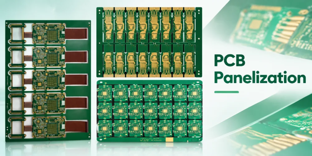
Imagine a 26 × 18 mm circuit that must pass through stencil printing and pick-and-place before it is separated into individual boards. A denser array might look cheaper in CAD, but it could be harder to support, inspect or depanel. That is the practical challenge behind small PCB panelization.
Here we build two arrays from the same hypothetical board: a 12-up arrangement and a 16-up arrangement. The arithmetic is simple; the engineering decision is not. Finished-edge condition, tooling rails, assembly support and shipping format can outweigh a small gain in geometric utilization.
The dimensions in the example are illustrative inputs, not Highleap standard process limits. For introductory terminology, see our Oversigt over printkortpanelering; the worked design below is intended for review by both the fabricator and the SMT assembler.
Indholdsfortegnelse
SMALL PCB PANELIZATION
Planning a Small PCB Array for SMT?
Share the PCB outline, assembly process, separation preference, quantity and handling constraints for a panelization review.
Request a Panelization Quote →Define the Panel’s Job Before Drawing the Array
Before drawing an array, establish where the boards will be handled as a joined group. Is the panel used only in PCB fabrication, through SMT reflow, through inspection, or even through shipment? These are not the same requirements. A bare-board fabricator may prefer one working-panel layout while an assembler needs smaller conveyable arrays with rails, fiducials and tooling holes. The eventual customer may need individual pieces with a clean, dimensionally controlled edge.
The board outline determines where temporary bridges can be added. A tiny optical-module PCB, for example, may have a connector contact edge, mounting holes, components close to the perimeter and an unusually thin substrate. None of those edges should automatically receive a breakaway tab. An approved no-tab zone may be necessary wherever a breakout remnant could affect the housing or mating connector. The underlying contact process is explained in fremstilling af hårdt guldfinger-PCB.
Collect six inputs before attempting the layout
| Input | Decision it enables |
|---|---|
| Finished PCB X/Y outline and tolerance | How many units fit, and which edges cannot tolerate a tab |
| Board thickness, material, copper distribution | Whether a scored line or routed web is feasible and how the joined array behaves mechanically |
| Components and connector overhang | Minimum neighbor clearance and forbidden rail positions |
| SMT equipment constraints | Panel conveyance direction, edge support, required fiducials and tooling |
| Separation method and acceptable edge condition | Tab location, V-score direction and post-separation inspection |
| Delivery state and lot identification | Whether rails remain, how many good circuits count as a shipment and how rejects are handled |
A production release should also identify who approves the final assembly array. If a design owner freezes panel rails without the assembler’s review, the resulting panel may be good for fabrication but poor for solder-paste printing or depaneling.
Worked Example: Compare a 12-Up and a 16-Up Array
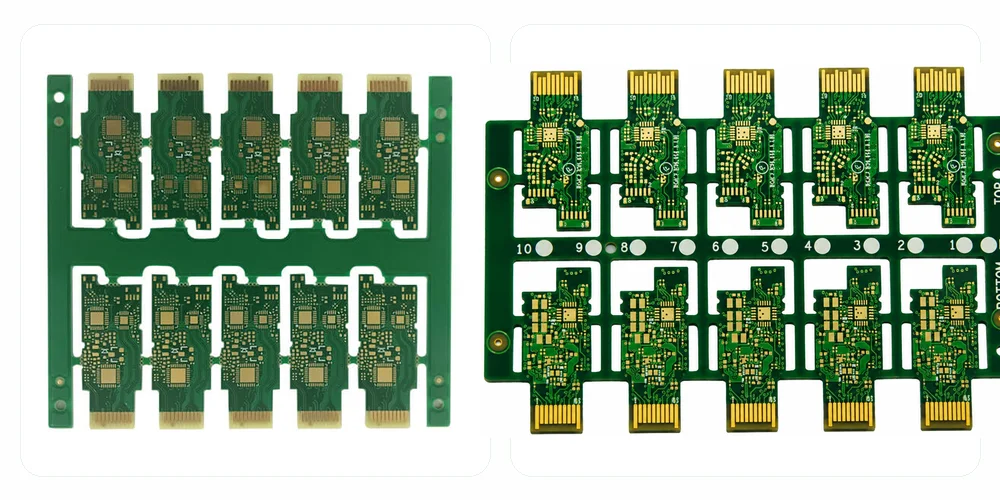
All dimensions below are assumptions for teaching the calculation—not claimed Highleap line limits or standard rail widths. Imagine a 26 mm × 18 mm control PCB. Suppose the assembler provisionally accepts an 8 mm handling rail on each side of a rectangular array, and the proposed routed-tab scheme needs a nominal 2 mm separation gap between neighboring board outlines. A gold contact on one 26 mm edge is designated as a no-tab/no-score edge. For simplicity, assume one board orientation for each proposal.
For a regular array of N columns and M rows, the outside envelope is:
Array width = N × board width + (N − 1) × inter-board gap + two side rails.
Array height = M × board height + (M − 1) × inter-board gap + two end rails.
The geometric board-area fraction is (N × M × single-board area) ÷ overall array-envelope area. This is only a layout indicator, not factory laminate utilization, because fabrication production panels, test coupons, tooling margins and process scrap are not included.
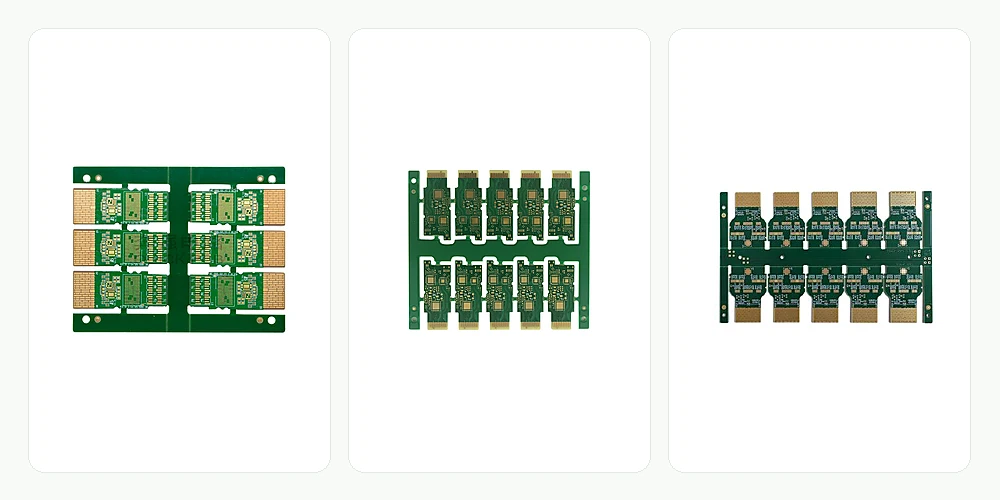
Candidate A: 3 columns × 4 rows, 12 circuits
- Width: 3 × 26 + 2 × 2 + 2 × 8 = 98 mm.
- Height: 4 × 18 + 3 × 2 + 2 × 8 = 94 mm.
- Overall rectangle: 98 × 94 = 9,212 mm².
- Twelve finished board areas: 12 × (26 × 18) = 5,616 mm².
- Geometric board-area fraction: 5,616 ÷ 9,212 ≈ 61.0%.
Candidate B: 4 columns × 4 rows, 16 circuits
- Width: 4 × 26 + 3 × 2 + 16 = 126 mm.
- Height: 4 × 18 + 3 × 2 + 16 = 94 mm.
- Overall rectangle: 126 × 94 = 11,844 mm².
- Sixteen finished board areas: 16 × 468 = 7,488 mm².
- Geometric board-area fraction: 7,488 ÷ 11,844 ≈ 63.2%.
| Beslutningsforanstaltning | 3 × 4 array | 4 × 4 array | What it actually tells us |
|---|---|---|---|
| Antal brædder | 12 | 16 | More circuits per array, not automatically more good circuits |
| Overall envelope | 98 × 94 mm | 126 × 94 mm | Must fit real conveyor and fixture envelope |
| Geometric board-area fraction | 61.0% | 63.2% | Slightly denser layout; not a cost quotation |
| Critical edge strategy | Skal gennemgås | Skal gennemgås | Contact edge must remain outside breakout or routing damage |
| Panel stiffness during handling | Kræver validering | Kræver validering | Longer lattices may flex depending on tab and rail structure |
| Estimated labor or SMT throughput | Ikke etableret | Ikke etableret | Needs equipment, cycle-time and test data |
Ingeniørmæssig konklusion: Candidate B uses the assumed rectangle slightly more efficiently, but this is not sufficient evidence to release it. Check whether 126 mm fits the approved conveyor and stencil support, whether the rail stiffness is sufficient through reflow, and whether the depaneling tool can access every break point. Candidate A may still be cheaper per accepted assembly if the wider panel raises defects or handling time. This distinction becomes central to volume-production panel optimization.
Select V-Scoring or Tab Routing by Edge Risk
There is no one best separation method for every small PCB. It depends on outline geometry, copper and component keep-out, material/thickness and the actual depaneling machine. This is especially important where modules fit into tightly controlled housings.
V-scoring: efficient only where the geometry permits it
V-score lines favor straight separation paths that can be supported by the manufacturer’s scoring process. They may reduce routed waste or handling steps for suitable rectangular boards. But a scored panel retains a controlled residual web and requires a compatible separation method. Flexing can impose strain on nearby solder joints or brittle components, so an assembly with edge-mounted ceramic capacitors or fine-pitch devices needs an explicit stress review. Score direction, line continuity, board construction, and acceptability of the finished edge should be approved—not assumed from a nominal score depth copied from another product.
Tab routing: more edge freedom, more local decisions
A routed outline with breakaway tabs can protect irregular or precision edges, but the designer must decide where each tab sits, how wide it is, what hole pattern (if any) is used and how the remaining witness/remnant is handled. A tab beside a card-edge contact can create an unacceptable protrusion after separation. Too many routed openings may also weaken the panel before SMT. A mouse-bite depanelization guide provides background on perforated tab treatments; final sizes must be approved against the actual shop and assembler capabilities.
Hybrid arrangements: possible, but not automatically simpler
Some designs combine straight scores on one axis with routing for special edges. A hybrid panel can be practical, but it increases the need for unambiguous drawings and compatible tooling. Do not specify such a combination merely to claim better utilization; it should solve a verified handling or edge-quality problem.
Need a Small-PCB Array Reviewed? Share the PCB outline, proposed array, assembly-rail needs and depaneling restrictions.
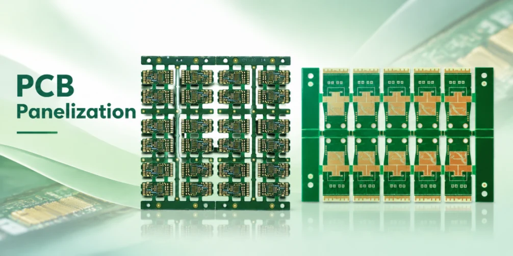
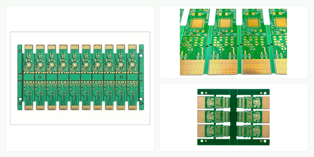
Small PCB panels for component assembly and separation
Design Tooling Rails and SMT Support Together
A rail is not just wasted laminate. It can be necessary for conveyor support, clamping and identification. But its location and dimensions must match the equipment that will print paste, place parts and inspect the assembly. Rails may carry panel fiducials, tooling holes, barcode/lot marks or test references; those features are not interchangeable.
Global fiducials help the placement system determine the array’s position and rotation. Lokale tillidspersoner, when required, improve recognition for specific fine-pitch operations. Tooling holes mechanically locate a panel in a fixture. The assembler should provide the count, coordinates and keep-out requirements—there is no sensible universal rail/fiducial template for every SMT line.
Panel stiffness deserves a direct check. The board may be small, but a perforated, largely routed 16-up array can behave differently from a solid rectangular panel. Consider where the underside can be supported during printing, where heat may cause temporary deformation, and how heavy connectors or multiple reflow passes change handling. Highleap’s SMT panelization requirements article covers those general assembly-side concerns; the decision here is to apply them to the specific small-board drawing.
Protect Critical Edges After Depaneling
For a pluggable optical module, a single small edge defect can matter disproportionately. The contact finger region might require precise registration and a final bevel; an uncontrolled breakaway tab or poor packing can damage that geometry. A sensible acceptance sequence is: inspect the panel for processing damage; depanel by the approved technique; inspect the critical edge for burrs, fiber breakout and tab remnants; verify any dimension identified as critical; then pack in a way that prevents contact-to-contact abrasion.
The acceptance drawing should say what final state is being measured. “No rough edges” is subjective. “No tab remnant on edge datum E1; inspect the finished connector profile per drawing MC-02” is closer to a usable requirement, provided the referenced drawing actually defines the geometry and measurement approach. Do not claim V-score is prohibited for every high-speed module PCB; the acceptable process is the one validated against its structure and connector envelope.
Panel drawing checklist: release the array as its own controlled item
- Single-circuit part number, revision and outline references.
- Array ID and revision, X-by-Y map, orientations and total finished array envelope.
- Approved spacing, rails, cutouts, tooling holes and fiducials.
- Proposed breakaway method, tab coordinates, no-tab/no-score edges and final edge conditions.
- SMT support/fixture assumptions and whether assembled boards stay in the panel for inspection or programming.
- Defective-position handling, identification and permitted delivery state.
- Who is authorized to approve array changes once production is qualified.
The last two points frequently get lost between fabrication and purchasing. An engineering drawing may say “12-up,” but a buyer may place a purchase order for 1,000 individual boards and expect complete 12-up arrays. The arithmetic and acceptance implications are explained in Levering og panelisering af PCB-sæt.
Release the Array Only After a Practical Comparison
Before committing to the 12-up or 16-up example, request an assembler review that covers conveyance, printing/stencil support, component overhang, AOI and depaneling equipment. Request a fabrication DFM review for routing clearances, rails, copper registration and any plating/contact edge. Then compare actual cycle-time estimates, expected accepted-board outputs, array costs and defect scenarios.
A useful final note is: “Array layout is approved for the stated fabricator and assembler process; changes to orientation, breakaway tabs, rails, critical edge or quantity per array require documented review.” This avoids treating a panel layout as an insignificant purchasing detail.
Small PCB Panelization FAQs
Does putting more tiny boards into a panel always reduce cost?
No. It may reduce handling per circuit or marginal layout waste, but it can increase routing work, stiffness problems, depaneling damage or reject exposure. Compare good units and production costs, not only the array count.
Should the PCB fabricator or the SMT assembler design the panel?
Both should review the requirements. The fabricator understands production panel and routing constraints; the assembler knows conveyor, stencil, reflow, inspection and depaneling conditions. The owner of the final array release should be identified in the purchase documentation.
Are standard rail dimensions or score depths safe to copy?
Treat them as provisional examples only. The board thickness, material, tool, component placement and equipment requirements determine what is acceptable.
Can gold-finger contacts be separated on a V-score line?
Only if the complete contact edge and connector mechanics are preserved by an approved process. A score line through a precision mating contact region should never be assumed acceptable without the interface and fabrication review.
Request a Small-PCB Panelization Review
Send the individual PCB data, outline and assembly constraints, existing panel proposal (if any), intended separation process and delivery quantity. A project-specific PCB manufacturing quotation can then identify missing panel-release information rather than silently assuming a generic 4 × 4 layout.

anbefalet Indlæg
Producent af optisk transceiver-printkort til brugerdefinerede pluggbare moduler
Highleap Electronics fremstiller og samler specialfremstillede...
Producent af optiske modul-printkort til 400G-, 800G- og 1.6T-programmer
Highleap Electronics leverer optisk modul PCB...
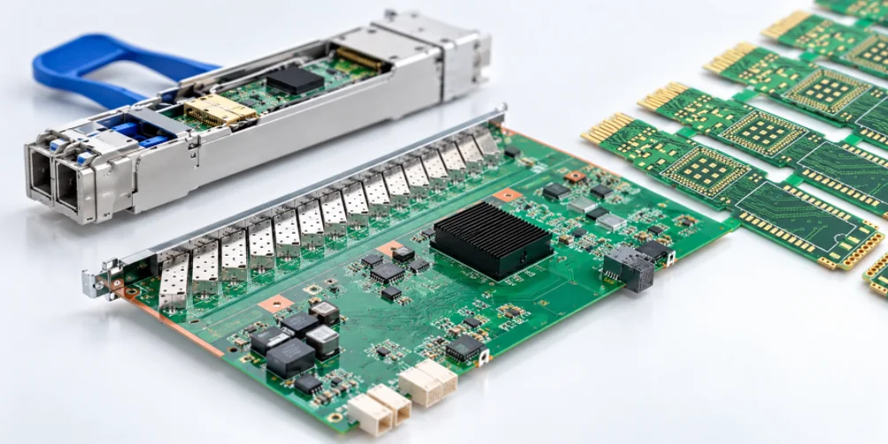
Producent af optisk kommunikations-PCB til fibernetværksudstyr
Highleap Electronics fremstiller og samler optiske...
Produktion af optisk transceiver-printkort i Kina
Highleap Electronics leverer optisk transceiver printkort...
Sådan får du et tilbud på printkort
Lad os køre en DFM/DFA-analyse for dig og vende tilbage til dig med en rapport. Du kan uploade dine filer sikkert via vores hjemmeside. Vi har brug for følgende oplysninger for at kunne give dig et tilbud:
-
- Gerber, ODB++ eller .pcb, spec.
- Stykliste, hvis du ønsker montering
- Antal
- Vendetid
Udover printkortproduktion tilbyder vi en omfattende vifte af elektroniske tjenester, herunder printkortdesign, printkortbaseret udstyrs ...
For PCBA-tjenester bedes du fremvise din BOM (Bill of Materials) og eventuelle specifikke monteringsinstruktioner. Vi tilbyder også DFM/DFA-analyse for at optimere dine designs med hensyn til fremstillingsevne og montering, hvilket sikrer en problemfri produktionsproces.