
PCB COST & QUOTATION
14層基板のコスト:製造、試作品、量産価格
14 layer PCB cost at Highleap Electronics is quoted against the released construction, manufacturing quantity and agreed acceptance criteria. Board outline and copper-layer count establish only part of the manufacturing cost. Laminate grade, finished thickness, drilling structures, impedance verification, specialized plating and inspection records can change the route substantially. We provide custom project quotations rather than an arbitrary unit price that does not correspond to a defined product.
ガーバーファイルまたはODB++ファイル、スタックアップ、目標数量、検査要件をお送りください。組立用の部品表(BOM)も追加してください。
14 Layer PCB Cost: What a Manufacturing Quote Includes

Highleap can quote a fourteen-layer board once the fabrication scope and quantities are identified. Its custom 14-layer PCB manufacturing service identifies the broader bare-board capabilities that establish the RFQ route. A quote based on only the layer count and board dimensions is a budget indication at best; it cannot account for low-loss dielectric, controlled-depth drilling, very small plated holes, inspection reports or a production-representative build. The released data are needed to distinguish factory setup from the recurring price of a finished board.
The following quotation worksheet is designed for practical supplier comparison. Leave a field explicitly “to be confirmed” if the designer has not released it. Do not allow different vendors to silently choose different materials or test scopes and then compare only the unit prices.
| 引用入力 | 必須の詳細 | Cost or schedule exposure if omitted |
|---|---|---|
| Bare-board quantity | Prototype, pilot and annual release quantity separately | Setup, panel yield and material buys differ |
| PCBの概要 | Finished dimensions, shape, panel or individual pieces | Production panel utilization and routing time |
| 材料 | Named dielectric/copper system or approved alternative | Unpriced low-loss or special material, procurement delays |
| 積み重ねる | Physical layer order, finished thickness and copper by layer | Re-engineering, via aspect ratio and press route |
| 相互接続 | Finished hole, blind/buried spans, microvia or VIPPO details | Additional drilling, filling and lamination operations |
| 電気的受容性 | Netlist electrical test, impedance coupon/report, sampling | Different test coverage and reporting costs |
| Finish and shipping | Solder finish, hard-gold region, packing, terms | Different processing, protection and freight scope |
Highleap’s general PCB製造サービス covers multilayer prototypes and production. For an accurate fourteen-layer commercial decision, the quoted process route and included verification documents should be compared line by line—not hidden inside a blanket “multilayer PCB cost” figure.
Can I obtain a 14-layer PCB price before the final stackup is approved?
A provisional estimate may be possible with stated assumptions, but it should not be treated as a firm production order. Board thickness, laminate, smallest hole, special via construction and impedance acceptance can each change fabrication cost. Ask Highleap to mark the unresolved items and update the quotation when the physical build and inspection scope are approved.
What fabrication operations are included in the quoted board price?
A complete bare-board quotation includes the approved board size and panel arrangement, fourteen copper images, selected cores and prepregs, lamination, drills and plated interconnects, finish, outline processing, electrical test and the specified inspection documentation. Tooling, CAM engineering, material minimum orders and any dedicated impedance coupon preparation may be treated separately or allocated across the ordered quantity. Both approaches can be valid, but the inclusions must be clear.
ハイリープの PCB fabrication cost information provides general pricing context. For fourteen layers, the accurate quote begins with the actual layer and drill data, not only the requested board dimensions. Copper distribution can change panel yield and resin requirements; an unusual profile can alter routability and array utilization; special test reports may require coupons and sampling that would not otherwise be included.
What is the price of one 14-layer PCB?
A fixed per-board price cannot be established from the layer count. The number of boards per manufacturing panel, approved laminate availability, exact vias, finish, tests and requested volume determine the result. The unit cost for an engineering lot also carries a larger share of process setup and data preparation than a repeat order. Highleap can quote multiple volume levels using the same drawing and clearly stated manufacturing assumptions.
Standard Through-Hole vs. HDI 14-Layer PCB Pricing
The most useful cost distinction is often 建設技術, not layer number. A conventional fourteen-layer board with standard plated through-holes can avoid special laser-drill build-up and filled-pad processes. A dense BGA design may need blind/buried via spans and microvias, and a high-speed card may require backdrilling or a specialty laminate. Those capabilities do not appear as a universal fixed-percentage surcharge: their costs depend on the exact drill and layer map, panel count and inspection plan.
| Build scenario (illustrative, not a Highleap customer quotation) | Principal operations | Specific RFQ decision |
|---|---|---|
| 14L standard PTH industrial controller | Conventional multilayer pressing, mechanical drilling, plated holes | Can standard laminate and routine test meet the design? |
| 14L high-speed network processor | Low-loss material, specified impedance, possible via-stub control | What are the insertion-loss and impedance deliverables? |
| 14L fine-pitch FPGA with HDI | Defined laser/buried via pairs, sequential build if required, VIPPO | Which BGA pads or layer pairs really require HDI? |
| 14L mixed high-current controller | Selective thicker copper, fine-line signal zones, insulation/thermal review | Can different copper weights avoid full-board heavy copper? |
The right engineering answer may be a different board area or layer allocation rather than a more elaborate process. If a routing change removes an HDI stage without compromising the electrical or mechanical requirements, the recurring manufacturing cost can improve. But forcing the design to avoid all blind vias may create additional layers, larger panels or unacceptable channel transitions.
14 Layer PCB Prototype, Pilot and Volume Cost Comparison
Engineering samples often prioritize validation of stackup, connectivity and assembly fit. The initial program may require more CAM discussions, first-article checks and small-quantity handling per board. Pilot builds establish the repeatable materials, factory route and inspection documents; volume releases benefit from consistent panelization and qualified stock planning, but still incur the contracted quality controls.
Cost comparisons should use one approved stackup and one revision. If the prototype is built with a substitute laminate or simplified hole structure that will not be repeated, its price does not establish the economics of production. A reliable 14-layer prototype-to-production plan keeps the sample route and future volume assumptions aligned, or documents exactly where they differ.
Does a larger order always lower the 14-layer PCB unit price?
Not without limits. Yield, material procurement minimums, bottleneck operations and agreed inspection can offset volume savings. A batch with many test coupons, difficult registration or special drilling might not show the same price reduction as a conventional through-via stack. It is more useful to request specified price breaks and their corresponding delivery schedules than to assume a fixed percentage discount.
How does panel utilization change a 14-layer PCB unit price?
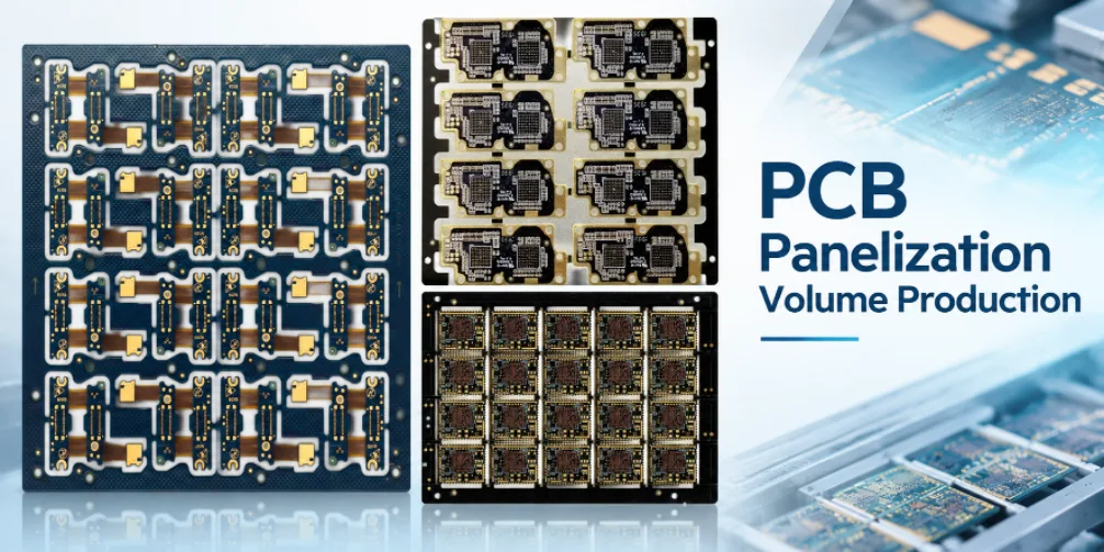
Panel utilization is the fraction of manufacturing area that becomes acceptable finished products. The calculation depends on the usable laminate panel, tooling margins, board outline, separation method, registration features and the need for coupons. A small irregular board can be less economical than a larger rectangular board if panel packing is poor. Conversely, a dense square board with a challenging via architecture may have high processing cost despite good nesting.
Ask the supplier to quote the intended delivery format—singulated boards or panels—and whether changing orientation, break-off rails or tooling-hole locations would improve production yield without changing the final mechanical interfaces. If the PCB is assembled, panelization must also work with SMT conveyors, printing, reflow support and final depaneling; the bare-board-only cheapest panel is not always the lowest delivered-PCBA cost.
Laminate, Stackup, Thickness and Panel Utilization Costs
Standard high-Tg FR-4 and specialty low-loss materials have different material costs and may require different manufacturing controls. The electrical channel budget, thermal exposure and approved material list should drive the choice. A low-loss laminate is not automatically required for all fourteen-layer designs, and the lowest-priced FR-4 grade is not an acceptable substitute for a qualified high-speed dielectric without review.
Finished board thickness has implications for press construction and mechanical drilling. The same fourteen layers in a constrained thin board may require tight dielectric control, while a thick board with small finished PTHs can raise aspect-ratio and plating concerns. Heavy copper regions affect inner-layer etch clearance, resin fill and stack symmetry. These are manufacturing costs caused by the design, not an arbitrary surcharge for fourteen layers. Our 14-layer stackup and material review documents these construction decisions before production.
Is 14-layer PCB fabrication always more expensive than a 12-layer board?
Not necessarily for two different designs. The additional copper layers and pressing operations often raise base cost under otherwise identical conditions, but a conventional fourteen-layer PTH board may still be simpler than a twelve-layer HDI board with multiple microvia stages. Compare like-for-like board area, laminate, via structure, finished thickness, tolerances and inspection scope. A percentage based only on layer count is not a defensible quotation.
Via-in-Pad, Backdrilling and Special-Process Charges
Blind/buried vias, laser-drilled microvias, filled and capped via-in-pad, depth-controlled backdrilling and special copper processes each have distinct cost drivers. A blind/buried architecture may alter lamination sequences and registration. Via-in-pad can require filling, planarization and copper cap plating, especially in fine-pitch BGA lands. Backdrilling needs depth control to remove unused barrel without damaging active internal layer connections.
These features should appear in the manufacturing files as explicit structures—not as generic notes saying “HDI board.” Highleap can evaluate a design-specific blind-via build (NAIST) と backdrilling operation to determine whether separate tooling, coupons or inspection is required. Deleting a special via may not save money if the alternative forces a larger board, longer high-speed route or different layer arrangement.
Use the same drawing, copper stackup, materials, test criteria and delivery terms for every quotation. Highleap can distinguish the fabrication, special-process and reporting items.
Electrical Testing, Impedance Coupons and Documentation Costs

A Class 2 or Class 3 statement alone does not define every report on a 14-layer order. IPC-6012 addresses rigid-board performance requirements and IPC-A-600 assists with visual acceptability, while the manufacturing package should set agreed sampling, coupons and extra customer tests. Additional scope such as cross-section analysis, thermal-stress qualification, controlled-impedance TDR reports, special substrate certificates, full serialization or first-article reports can influence setup, throughput and the released-board price.
Do not pay for a generic report title without defining its acceptance purpose. Netlist testing addresses open/short defects; an impedance coupon measures its prescribed transmission line; microsection inspection addresses selected plated structure conditions. None substitutes for testing the populated electronic product. In a high-reliability program, request the actual report format and lot traceability resolution before deciding which quotation has more complete coverage.
Are impedance coupons included automatically with every fourteen-layer order?
No universal assumption is appropriate. If the drawing specifies controlled impedance, confirm which target, tolerance, coupon structure, panel sampling and result format are included. Even when a factory routinely makes impedance-controlled boards, the acceptance evidence for a particular program may require separate engineering and reporting work.
How are impedance coupons and related quality records priced?
An impedance-controlled fourteen-layer PCB may require a stackup field solution, representative coupons, TDR measurements and defined records. These are not interchangeable with an ordinary bare-board continuity/isolation test. Additional structural requirements—for example plated-hole microsections, specific thermal-stress sampling or lot traceability—should be included in the RFQ if required.
For comparison, specify the applicable IPC rigid-board class, test scope, sampling method and whether reports accompany each shipment. Where a quote says “100% tested,” confirm 何 is tested: all nets for continuity and shorts, designated coupons for impedance, or something else. Highleap can align the offer with its PCB electrical-test procedures, subject to project-specific requirements.
Why can two manufacturers quote different prices for the same 14-layer drawing?
The manufacturers may be using different assumed laminate grades, panel yield, drill limits, inspection coverage, outsourcing routes or commercial terms. One price may include tooling and impedance documentation, while another excludes them. A price comparison is meaningful only after differences and proposed substitutions are reviewed and the same acceptance package is confirmed.
What is the true cost of a late engineering change?
A late change may force new CAM work, new tooling or film, different laminate, another set of impedance calculations, a replacement prototype and new inspection. On an assembled network or FPGA board, that revision can also require a stencil change, rework or scrapping of purchased components. For a fair total-cost evaluation, include the likelihood and ownership of such changes, not only the first bare-board unit price.
For programs expected to move into recurring production, request two prices for the same construction: one for engineering samples and one for the forecast production lot. Separately identify one-time setup, material commitments and agreed remaining-stock treatment. The sampling and test scope should not quietly disappear from the volume quotation.
Comparing China 14-Layer PCB Quotes and Total Delivered Cost
| 商業的要素 | Verify in both quotations |
|---|---|
| 材料とスタック | Approved laminate grade, thickness, copper by layer and permitted substitutes |
| インターコネクト | Drill sizes, via spans, backdrill, fill/cap and relevant tolerances |
| 品質 | IPC class, e-test, coupons and specified inspection evidence |
| 供給 | Tooling, price breaks, delivery terms, volume plan and exceptions |
確認する 物理的な積み重ね, including material grades and dielectric construction; the interconnect package, including finished holes and special processes; the acceptance deliverables, including standards and coupon records; and the commercial boundary, including quantities, tooling, delivery terms and responsibility for changes. Highleap can identify quotation assumptions and exceptions during DFM so the approved purchase order describes the actual board.
International supply decisions can also depend on logistics, import terms, material continuity and communication around engineering changes. For China-based sourcing, our PCB manufacturer qualification information supports supplier comparisons without relying on price alone.
Which costs belong in a China supplier comparison?
For international shipments, a delivered-board comparison includes the supplier’s stated shipping terms, export packing, customs/documentation responsibilities, destination and delivery format. Currency, tariff classification and local taxes are project-dependent and should not be guessed from the layer count or a website offer. Price quotations should state the actual Incoterm and whether freight, tooling, special inspection and component procurement are in the same currency and validity period.
Supplier risk can also become cost. An unapproved laminate change may invalidate a high-speed test, a missing X-ray plan can delay assembly qualification, and uncertain ownership of excess BOM materials can create unplanned charges. Highleap can supply a coordinated fabrication/PCBA quotation, but the separate costs and responsibilities should remain identifiable. That makes repeat purchasing easier to audit and helps compare a China-based manufacturer against an alternative without using unsupported claims of guaranteed percentage savings.
Does consolidating PCB fabrication and assembly always reduce cost?
No. Consolidation can reduce coordination work and expose incompatibilities earlier, especially around BGA via fill, finish and panelization. Whether it produces a lower total price depends on component procurement, setup allocation, test requirements, transportation and the customer’s existing suppliers. Compare a complete tested-PCBA price against the same deliverable—not bare-board pricing against an integrated assembly quote.
14 Layer PCB Assembly Cost vs. Bare-Board Pricing

A bare-board unit price is different from a tested, populated PCBA price. An assembled FPGA or network card can carry a component BOM much more expensive than the substrate; programming fixtures, BGA X-ray requirements and functional-test duration add further costs. Highleap can prepare a combined 14-layer PCB and SMT assembly quotation that separates board fabrication, approved components, placement, programming, testing and packing.
For this combined quote, provide the fabrication data plus an approved BOM with manufacturer part numbers, centroid file, assembly notes and required test procedure. Component alternatives require engineering approval; a quoted substitution should not silently change a qualified product.
Request a Detailed 14 Layer PCB Price
Send Gerber/ODB++/IPC-2581, mechanical and drill files, stackup, finished copper and thickness, impedance requirements, special via drawings, finish, order quantities, inspection standard and the delivery destination. Highleap can return a quotation against defined manufacturing conditions, with tooling, optional reports and assembled-board scope distinguished where appropriate.
Submit quantities, layer construction, material grade, special features and the required acceptance records.
Share the complete board data with prototype and production quantities. We can quote against the agreed material and via construction, rather than a made-up price per layer.

おすすめの投稿
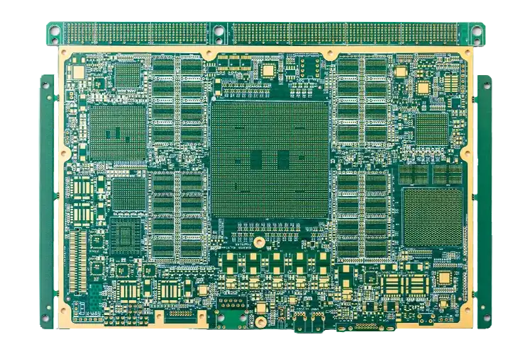
中国の14層基板メーカー
カスタムリジッド多層基板 Highleap Electronics...
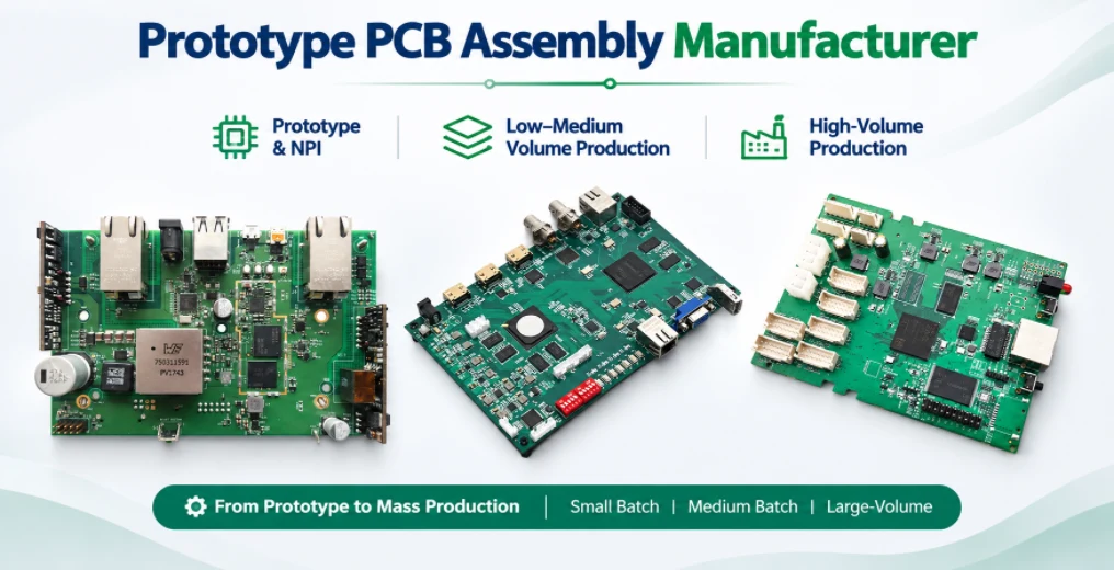
14層基板アセンブリとワンストップ基板製造
PCB製造+PCBA Highleap Electronicsは14のサービスを提供しています。

高熱性能電子機器向けAlNセラミック基板メーカー
ハイラップ・エレクトロニクス社製・窒化アルミニウムセラミック基板…

OEM試作品および量産向けアルミナ基板製造
ハイラップ・エレクトロニクス · アルミナセラミック基板製造...
PCBの見積もりを取得する方法
DFM/DFA分析を実施し、レポートをお送りいたします。ファイルは当社のウェブサイトから安全にアップロードできます。お見積もりには以下の情報が必要です。
-
- Gerber、ODB++、または .pcb 仕様。
- 組み立てが必要な場合のBOMリスト
- 数量
- ターンタイム
PCB製造に加え、PCB設計、PCBA、ターンキーソリューションなど、包括的な電子サービスも提供しています。試作、設計検証、部品調達、量産など、お客様のプロジェクトを成功に導くエンドツーエンドのサポートをご提供いたします。
PCBAサービスをご利用の場合は、BOM(部品表)と具体的な組立指示書をご提出ください。また、DFM/DFA解析により、製造性と組立性を最適化し、スムーズな製造プロセスを実現します。