
CUSTOM RIGID MULTILAYER PCB
14-laags PCB-fabrikant in China
Highleap Electronics manufactures custom 14-layer rigid PCBs in China and coordinates PCB assembly for OEM electronic equipment. Our manufacturing scope encompasses conventional through-hole multilayer boards and, following design review, constructions involving controlled impedance, fine-line routing, blind or buried vias, via-in-pad, backdrilling, special copper distribution and different surface finishes. Fabrication is released against the approved manufacturing drawing, not against layer count alone.
Send your Gerber or ODB++ files, stackup, target quantity and inspection requirements. Add the BOM for assembly.
Fourteen-layer circuit boards are supplied for networking equipment, industrial controllers, FPGA carrier boards, embedded computing, measurement systems and high-density communication electronics. Highleap can provide a coordinated fabrication and assembly quotation covering PCB construction, approved components, SMT/THT processing and the inspection or functional tests specified for the order. Our wider Productiemogelijkheden voor meerlaagse printplaten support the same build-to-print approach.
14 Layer PCB Manufacturer in China: Capabilities and Fabrication Scope
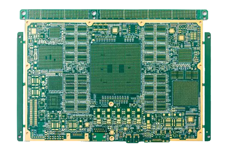
Highleap Electronics is a China-based PCB fabrication and electronics assembly provider. Our published rigid PCB manufacturing capability table lists multilayer rigid construction up to 60 lagen, with fine-line imaging, mechanically and laser-drilled interconnects, controlled impedance and several surface-finishing options. A fourteen-layer rigid board is therefore within the company’s stated layer-count envelope. The publicly listed figures are portfolio-level capabilities, not a guarantee that every maximum can be combined in a single stackup.
For accurate vendor qualification, the manufacturing offer is tied to a drawing. A 14-layer board using standard through holes and commercially stocked FR-4 is different from a fourteen-layer board combining 2/2 mil traces, very small mechanical holes, heavy inner-layer copper and specialty low-loss materials. Highleap reviews the actual stackup, finished thickness, smallest hole and plating requirement, dielectric, trace geometry, assembly interface and target lot quantities before confirming manufacturability.
| Published rigid-PCB capability | Highleap’s publicly stated range | What is decided for this 14-layer order |
|---|---|---|
| Meerlaagse constructie | Up to 60 rigid copper layers | Final approved 14-layer construction and production site |
| Fijne lijncircuits | Down to 2/2 mil as a portfolio capability | Selected layers, finished copper weight, allowed etch tolerance and production margin |
| Mechanisch en laserboren | Specialized small-hole and HDI capabilities published | Exact drill diameter, hole aspect ratio, microvia span and interconnection reliability |
| Copper and specialty finishes | Heavy-copper and ENIG/ENEPIG/hard-gold capabilities listed | Copper-by-layer matrix, finished finish thickness and which pads use each finish |
| Gecontroleerde impedantie | Published manufacturing and coupon-test support | The approved impedance matrix, stackup, coupon geometry and lot acceptance report |
Highleap's PCB-fabricageservice en factory equipment overview provide further company-published context. The specification on the quotation, approved stackup and named manufacturing route should take precedence over any general marketing table. This distinction lets project teams compare suppliers on a testable engineering package rather than a list of unrelated maximum figures.
Can Highleap confirm a nonstandard fourteen-layer build before an order?
Yes, after receiving the build data. The response can identify the proposed press construction, alternative material if the requested grade is unavailable, drill or routing issues, intended test coupons and any exception needing written approval. If a combination falls outside the approved process window, it should be redesigned or specifically qualified rather than described as a standard 14-layer capability.
Which 14-layer PCB manufacturing capabilities can be combined?
A fourteen-copper-layer construction requires a controlled sequence of inner-layer imaging, lamination, drilling, plating and final finishing. Before fabrication, Highleap reviews the layer order, finished board thickness, conductor copper weight, laminate type, trace and spacing constraints, hole aspect ratio and special features. The approved proposal identifies the actual material system and construction route rather than treating a generic capability-table maximum as a blanket approval.
In a conventional 14-layer through-hole board, mechanically drilled holes connect selected layers or pass through the structure as designed. For dense escape routing, blind and buried vias may be considered; sequential lamination is associated with the particular via architecture rather than the number fourteen. Microvias, stacked or staggered interconnects and capped via-in-pad each add their own construction and inspection requirements. Highleap reviews the HDI fabrication options against the hole map and laminate details when a conventional route does not meet the design.
The standard fabrication package should include the outline drawing, Gerber or ODB++/IPC-2581 data, NC drill files, layer map, finished copper requirements, solder mask and legend, finish definition and acceptance specification. For impedance-controlled nets, include a layer-indexed impedance table and the desired verification method.
Can Highleap fabricate 14-layer PCBs with controlled impedance?
Yes, within a design-specific approved stackup and test plan. The trace cross-section depends on finished copper, dielectric thickness, material properties and the actual reference planes. Highleap can review target single-ended and differential impedance, propose manufacturable adjustments and quote appropriate coupons or measurement records when specified. Published general tolerances must not be assumed to apply to every conductor geometry without confirming the proposed stackup.
What information should be provided for a manufacturer capability check?
Zorgen voor physical finished size and thickness; all fourteen copper layers; the drill map with plated, unplated, blind/buried and backdrill features; copper weight per layer; material preference; minimum trace/space by layer; solderable or contact finish zones; impedance table; required IPC class; and annual quantities. Highlight the single most critical requirement: for example, a 0.8 mm-pitch BGA escape, a tight connector finished-hole tolerance, an RF loss budget or a high-voltage spacing requirement. With these details Highleap can respond to the engineering problem that actually controls yield.
The company can quote prototypes and recurring builds under one released drawing, with the exception and substitution process specified up front. The final factory and test scope for an individual customer program are confirmed in the commercial and manufacturing documentation, not inferred from a website’s full portfolio.
Custom 14 Layer PCBs for Networking, FPGA and Industrial Electronics
A 14-layer network switch PCB may carry high-speed serial interfaces, clock distribution, power rails and complex connectors. Layer planning is driven by differential channel routing, return-path continuity and insertion-loss constraints. Backdrilling may be necessary for selected plated-through-hole stubs, whereas a different networking product may meet its channel requirement without the extra operation.
In FPGA and embedded-computing carrier boards, BGA escape often dominates the routing decision. The relevant constraints are pad pitch, escape channel width, via structure, available reference planes and board thickness. High-density signal routing can also affect assembly choices: solderable pad finish, panel support, BGA inspection access and board flatness must be considered together.
Industrial automation PCB projects bring different requirements. Processor and Ethernet sections may sit alongside isolated inputs, motor-control interfaces, precision analog acquisition and press-fit connectors. Copper planes and creepage or clearance constraints follow the electrical design, not an assumed standardized 14-layer arrangement.
Het high-speed PCB manufacturing service addresses controlled dielectrics, channel loss and fabrication details for designs where signal performance governs the stackup. A detailed 14-layer stackup review is available for the physical layer assignment and material selection.
Which related fourteen-layer board types can Highleap review?
A fourteen-layer PCB can be the main controller in a larger electronic assembly. Highleap can consider 14-layer industrial control PCBs, Ethernet switch and router boards, 14-layer FPGA and SoC carrier boards, network appliance mainboards, data acquisition cards, vision-system processor boards, embedded computer interface boards, telecom equipment cards and mixed-signal instrumentation. The board technology for each family is determined by the BOM, electrical interfaces and connector specification.
Networking and data communication: controlled-impedance pairs, continuous reference planes, connector transitions and possible backdrilling receive priority. Send a channel allocation and any insertion-loss test requirements. A board used in a network switch is not automatically a compliant high-speed channel simply because it has fourteen layers.
FPGA and computing carrier boards: BGA pitch, pad diameter, escape geometry, power-rail distribution and board flatness dominate the engineering review. With a dense FPGA, a 14-layer through-hole structure may be sufficient; where it is not, microvias or filled via-in-pad can be considered. The requested technology must follow the pin field rather than a generic layer-count rule.
Industrial control and instrumentation: processors and communication circuits can sit alongside isolated I/O, analog front ends and power conversion. Creepage/clearance, selective heavy copper, isolation barriers, press-fit connectors or vibration-sensitive hardware may control the build more than ultra-fine tracks. The drawing should identify the applicable insulation and mechanical acceptance requirements.
Power-monitoring and mixed high-current boards: separate copper weights and placement of thermal vias may be more practical than making all fourteen layers heavy copper. Finished copper, etch allowances, local resin volume and assembly thermal loading require a combined review. Designs seeking an alternative to a rigid fourteen-layer construction can also be assessed within Highleap’s wider multilayer and rigid-flex portfolio.
Can Highleap manufacture related boards as one matched product family?
The project can be scoped as a main fourteen-layer processor PCB plus related I/O, power, sensor or connector daughterboards. Keep each board’s part number, electrical test and approved revision distinct, while coordinating material purchasing, assembly and shipment identification at program level. A shared delivery date does not imply every PCB uses the same laminate, inspection method or production line.
Advanced 14-Layer PCB Fabrication: HDI, VIPPO and Backdrilling
Highleap can evaluate feature combinations that extend beyond a conventional fourteen-layer FR-4 board. Available routing and assembly interfaces may include blind and buried vias; laser-drilled microvias; resin-filled or copper-filled vias; plated-over via-in-pad; controlled-depth backdrilling; heavy copper planes; press-fit holes; countersinks or controlled-depth milling; edge contacts with hard gold; and different solderable pad finishes. Each option is assessed against its location and purpose on the customer drawing.
Via-in-pad is appropriate where a component escape route or thermal pad structure calls for a via directly in the solderable land. The fill, planarization and copper cap must be compatible with the package and the finished pad specification. Backdrilling serves a different purpose: it removes an unused length of plated-through-hole barrel while protecting required interconnections. The two processes should not be treated as interchangeable cost additions. Detailed tolerances and inspection depend on the approved via-in-pad construction en backdrill requirements.
A fourteen-layer PCB can also combine selected high-current copper regions with finer signal layers, but finished copper thickness, etching clearance and resin filling must be evaluated together. Similarly, an ENIG-finished SMT area and a hard-gold edge connector require separate plating definitions. When special features affect different layers or product regions, the fabrication drawing should call out the applicable area and inspection standard directly.
Does a 14-layer board automatically require HDI?
No. Fourteen layers describe the number of conductive copper layers. Standard multilayer fabrication with through-holes can satisfy many industrial and computing designs. HDI is specified when the required interconnect density, microvia span or component escape geometry justifies the additional processing.
What makes a special-feature 14-layer PCB difficult to quote correctly?
De wisselwerking between features is more important than the number of options listed. For example, a thick board with a small mechanical drill increases aspect-ratio difficulty; a copper-filled via beneath a fine-pitch BGA requires a sufficiently planar solderable cap; a hard-gold finger needs a different thickness and bevel callout from an ENIG SMT land; and backdrilling is only useful where the layer map and data channel justify removing an unused barrel. A quote should identify the manufacturing sequence and separately approved inspection criteria for these features.
Ask the fabricator to return a short manufacturing exceptions list. Material substitutions, pad-finish changes and modifications to via layers or annular rings should be treated as engineering changes. They can affect signal integrity or component assembly even if a revised board still passes a basic netlist electrical test.
PCB Materials, Finished Thickness and Stackup Approval
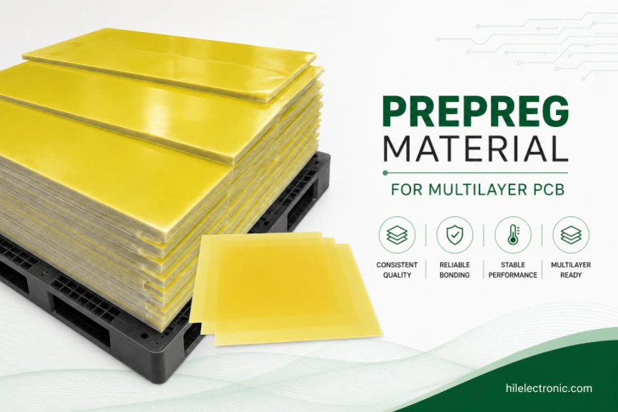
High-Tg FR-4, low-loss laminate and hybrid constructions are not equivalent substitutions. Tg indicates a thermal material characteristic; high-speed channel performance depends on dielectric loss, Dk, copper roughness, trace geometry and transitions. Material choice should follow the electrical and reliability requirements, the approved stackup and stocked or obtainable grades. Highleap can review high-layer-count laminate choices as part of the fabrication release.
Neither 1.6 mm nor 2.0 mm is a universal finished thickness for 14-layer PCBs. The appropriate thickness follows the layer dielectric requirements, connector fit, mechanical mounting and drill aspect ratios. The physical stackup must document the proposed cores/prepregs, finished copper by layer, critical dielectric spacing and final thickness tolerance. If the PCB is to be assembled, the expected reflow profile and flatness requirement are also relevant.
Changes to approved dielectric thickness, resin system or copper profile may alter impedance, plating or thermal behavior. Material alternatives should therefore be reviewed and authorized before manufacture rather than being silently substituted in response to stock shortages.
Send your stackup, copper/drill files, special-feature drawing and quantity. We can review the proposed construction and the inspection scope before quoting.
Supplier Qualification and Manufacturing Evidence
A trustworthy 14-layer PCB manufacturer should be able to discuss how it will verify your board, not merely offer an attractive capability badge. Highleap’s company site describes a multilayer fabrication facility, AOI and electrical testing, and a coordinated PCB/EMS service model. These are useful starting points for supplier evaluation; orders requiring formal qualification should also request the current certificate for the actual legal entity and production site, the scope of covered processes, and a sample of the relevant production records.
| Bewijsmateriaal om aan te vragen | Wat het aantoont | Grens van het bewijs |
|---|---|---|
| Manufacturing stackup approval | Approved material, press build and copper geometry | Not proof of finished channel performance without tests |
| Inner-layer AOI and layer registration records | Controls at stages not visible after lamination | Not a substitute for plated-hole acceptance |
| Plating microsection or coupon, if specified | Selected cross-sectional interconnect characteristics | A sampled structure, not every via in every board |
| Bare-board netlist electrical test | Open/short conformance for the fabricated circuit | Does not verify impedance, firmware or PCBA function |
| Impedance coupon and TDR records, if specified | Defined trace/coupon result under a stated tolerance | Not end-to-end insertion-loss or EMC certification |
| Lot identity, exceptions and certificate scope | Traceability and the actual site / documentation basis | Does not automatically certify the finished OEM product |
For higher-reliability electronics, specify the appropriate IPC-6012 edition and performance class along with IPC-A-600 acceptance expectations and any applicable customer addendum. Industry labels such as medical or automotive are not a substitute for a board drawing, exact acceptance plan and validated factory qualification. Avoid assuming Class 3, IATF or medical-device coverage applies to every order without checking the nominated site and certificate.
What would make Highleap an auditable candidate for a fourteen-layer PCB program?
A complete response should include a manufacturable stackup, an exception-free or explicitly qualified hole/copper construction, an inspection plan, unambiguous material substitution rules, a quotation covering the requested evidence, and a path from sample to repeat production. Request examples of redacted inspection reports and coupon records if the contract requires them. Public marketing information establishes an initial supplier profile; project-specific evidence is what supports final approval.
14 Layer PCB Inspection, Electrical Testing and Quality Records

Quality verification begins before lamination. Inner-layer AOI and registration checks are relevant because copper artwork faults become inaccessible after pressing. Subsequent checks address drilling, plating integrity, plated-hole condition, conductor spacing, finished outline, mask and solderable finish. Netlist-based electrical testing confirms bare-board continuity and isolation; it does not establish impedance or the function of a populated assembly.
Highleap can scope controlled-impedance coupon measurement, selected microsection inspection, first-article checks and lot records with the order. The acceptance plan should identify the applicable IPC-6012 rigid-board performance class, any IPC-A-600 visual acceptance criteria, approved deviations and required reports. Specific environmental or destructive tests should be quoted separately where they are required.
What test evidence can accompany a 14-layer PCB order?
The deliverable can include agreed electrical-test acceptance, dimensional inspection, specified impedance coupon data and selected plated-hole evidence. The exact test method, sampling, report format and retention requirements must be stated on the purchase package. No bare-board test should be represented as a guarantee of complete populated-board signal integrity or end-equipment qualification.
14 Layer PCB Fabrication and Assembly Under One Program

Highleap can coordinate bare-board fabrication, approved component procurement, SMT/THT assembly, programming and project-defined functional testing. The bare PCB should be released with assembly data early enough to verify BGA pads, via caps, connector holes, panel support and finished-surface compatibility. A board can pass fabrication inspection yet require an expensive change if these interfaces were left unresolved.
For populated equipment boards, our turnkey 14-layer PCBA service covers sourcing responsibility, BGA/QFN inspection, mixed technology, firmware and customer test requirements in detail. Full turnkey, partial turnkey and consigned builds remain distinct commercial models; component substitutions and other engineering changes follow the customer’s approval procedure.
China PCB Supply, Engineering Changes and Export Delivery
Highleap’s China-based manufacturing and EMS offering is positioned for international OEM and contract-manufacturing projects. For repeat deliveries to European, Israeli or other overseas engineering teams, the practical commercial details should be agreed before the first purchase order: Incoterms, packing and moisture/ESD handling as applicable, revision and label language, inspection documents, shipment split, delivery destination and the person authorized to approve a manufacturing change.
A supplier-managed project can coordinate the bare boards and separately priced PCBA, but the release should name the actual responsible parties for sourcing, PCB fabrication, component assembly and product-specific testing. The customer must retain approval authority for material changes, substitute ICs, altered board geometry and equivalent-surface-finish proposals. Where customer data are controlled, agree handling and access restrictions before file transfer.
The advantages of a China-based fourteen-layer source are meaningful only if the finished board meets its approved electrical/mechanical requirements and arrives with the promised evidence. A useful international supplier relationship is built on documented exceptions and repeatable revisions, not unsupported claims of zero defects, universally guaranteed lead times or certification of every end product.
Can fabrication and assembly be included in the same purchase order?
Yes, if the agreement explicitly covers bare-board acceptance, BOM ownership, stencil and assembly process, programming, functional testing, packaging and lot traceability. Highleap’s PCB-montageservice describes the broader EMS scope. The detailed PCBA release differs from the bare-board acceptance, and the two should be approved independently even under one commercial order.
Vraag een offerte aan voor de productie van een 14-laags printplaat.
Highleap can quote prototype, pilot and repeat-production quantities against a consistent engineering package. Send the current board data, 14-layer layer map, proposed material/stackup or fixed impedance targets, final board thickness, drill and special-feature drawings, surface finish, quantities, delivery destination and requested inspection documents. The production forecast is useful for evaluating material continuity and panel utilization.
Gedetailleerd pricing and cost variables en prototype-to-production release requirements can be reviewed separately without mixing pricing assumptions into the fabrication specification. A manufacturing quotation is released after significant technical exceptions and material substitutions have been defined and approved.
Upload the released fabrication data and identify any controlled-impedance, HDI, finish, test or assembly requirements. The quote will state the agreed manufacturing route and deliverables.

aanbevolen berichten

Fabrikant van Al2O3 keramische printplaten voor precisiekeramische circuits
HIGHLEAP ELECTRONICS · Aluminiumoxide keramische printplaat...
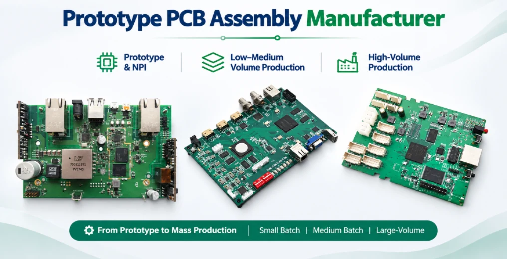
Fabrikant van prototype printplaatassemblages
Highleap Electronics is een prototype printplaatassemblage...
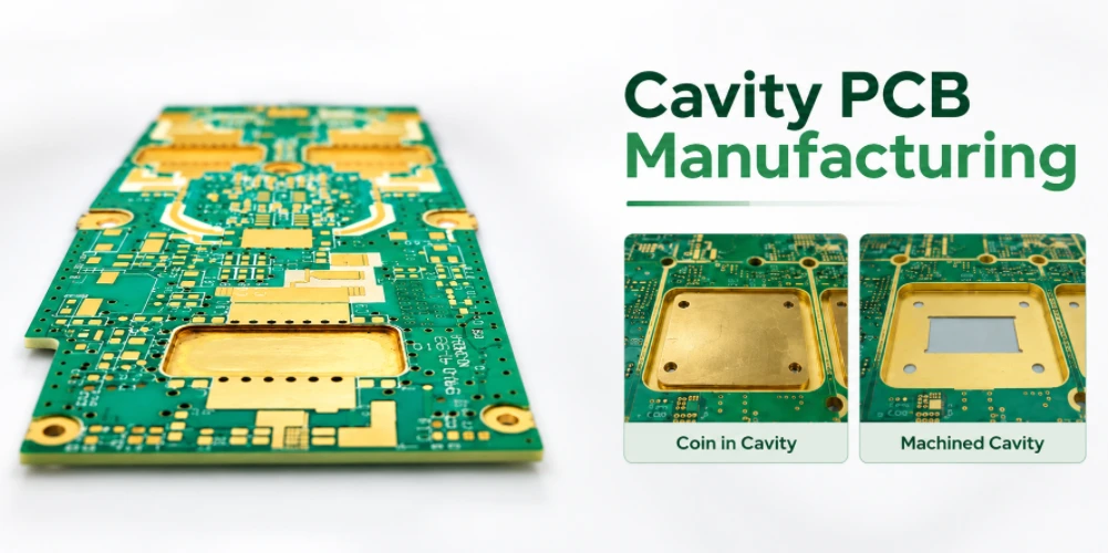
Printplaten met speciale functies voor OEM-producten
Highleap Elektronica / PCB + PCBA...
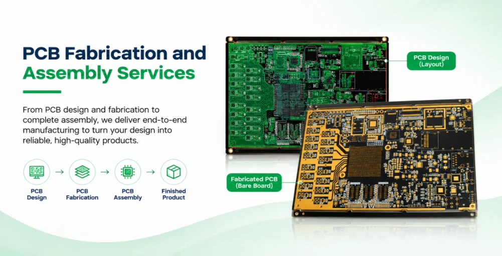
PCB-fabricage en -assemblage
Highleap Electronics verzorgt de fabricage en assemblage van printplaten...
Hoe u een offerte voor PCB's kunt krijgen
We voeren een DFM/DFA-analyse voor u uit en sturen u een rapport. U kunt uw bestanden veilig uploaden via onze website. We hebben de volgende informatie nodig om u een offerte te kunnen sturen:
-
- Gerber, ODB++ of .pcb, spec.
- BOM-lijst als u assemblage nodig heeft
- Aantal
- Draaitijd
Naast PCB-productie bieden we een uitgebreid scala aan elektronische diensten, waaronder PCB-ontwerp, PCBA en kant-en-klare oplossingen. Of u nu hulp nodig heeft bij prototyping, ontwerpverificatie, componentsourcing of massaproductie, wij bieden end-to-end ondersteuning om het succes van uw project te garanderen.
Voor PCBA-diensten verzoeken wij u uw BOM (Bill of Materials) en eventuele specifieke assemblage-instructies te verstrekken. Wij bieden ook DFM/DFA-analyses aan om uw ontwerpen te optimaliseren voor maakbaarheid en assemblage, wat een soepel productieproces garandeert.