
Snelle productie van 6-laags printplaten in China
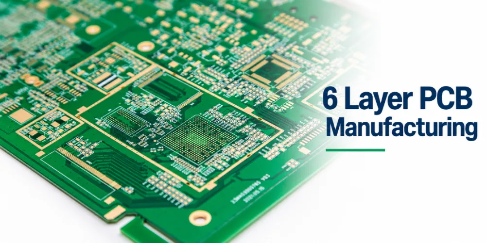
Highleap Electronics manufactures six-layer printed circuit boards for electronic products that require additional routing capacity, carefully planned reference planes and defined electrical and mechanical specifications. Quotes are based on the actual fabrication data, including laminate grade, stackup, copper weights, finished thickness, via structure, surface finish and special processing requirements.
Whether you are preparing a prototype, transferring an approved design to production or sourcing bare boards and assembled PCBAs, the quotation needs to reflect the actual construction—not just the number of layers. Submit your current design files and order requirements so the manufacturing scope, technical questions and pricing can be reviewed together.
Explore 6 Layer PCB Requirements
Have Your PCB Files Ready?
Send your Gerber files, stackup, quantity and required specifications to request a project-specific quotation.
Special materials and process requirements are subject to engineering review.
6 Layer PCB Types and Manufacturing Options
A six-layer PCB can have very different manufacturing requirements depending on its construction, materials, electrical specifications and mechanical features. Two boards with the same layer count and dimensions may require different production processes because one uses a standard plated-through-hole construction while the other includes gold fingers, controlled-depth machining, edge metallization or other special features.
The layer count alone is not enough to determine an accurate PCB quotation. Highleap reviews the fabrication data to assess board geometry, layer structure, drilling requirements, surface finish and any special processes. The following options identify the main requirements to define when sourcing a six-layer PCB.
Boardconstructie
- Six-layer rigid PCB
- High-density multilayer PCB designs
- Six-layer flex or rigid-flex constructions, subject to capability review
- Special multilayer constructions, subject to engineering approval
Layer count, board construction and interconnection requirements should be specified separately because they affect the manufacturing route.
Materials and Electrical Requirements
- Standard FR-4 laminate
- High-Tg and specified halogen-free materials
- High-speed and low-loss laminate systems
- Selected Rogers, PTFE or other specified grades, subject to review
- Gecontroleerde impedantievereisten
Specify the exact laminate grade when it is mandatory. Any proposed substitution should be evaluated against the project’s electrical, thermal and reliability requirements.
Copper and Mechanical Specifications
- Individual copper weights by layer
- Specified finished board thickness
- Fine-line and fine-spacing layouts
- Heavy-copper requirements, subject to review
- Special outlines, cutouts and dimensional tolerances
Finished dimensions, copper requirements and tolerances affect material usage, processing and inspection. Include specified values rather than relying on nominal dimensions alone.
Drilling, Slots and Interconnection
- Vergulde doorgaande gaten
- Blind and buried vias, where supported
- Via filling or plugging, where supported
- Controlled-depth slots and blind slots, subject to review
- Backdrilling and specified hole tolerances
Hole depth, slot geometry, remaining material thickness and plating requirements may change the process route. Identify these features in the manufacturing data and drawings.
Gold Fingers and Edge Features
- Gold-finger edge contacts
- Different finger lengths or contact areas
- Segmented or selectively arranged gold fingers
- Bevel requirements, where applicable
- Board-edge metallization and plated edge features, subject to review
Finger layout, plating requirements, contact dimensions, bevels and edge-metal details need to be clearly defined because different edge-contact designs may require different finishing processes.
Surface Finish, Inspection and Orders
- ENIG, OSP and other specified surface finishes
- Lead-free HASL where appropriate
- Testen van elektrische continuïteit en isolatie
- Impedance verification and reports when required
- Prototype, low-volume and repeat production orders
- Bare PCB supply or fabrication with assembly
Specify the required finish for the relevant contact areas, inspection criteria and order quantity so the quotation covers the intended product.
Why Gerber Files Are Important for a 6 Layer PCB Quote
Gerber files define the copper patterns, solder mask, legend and other fabrication layers needed to understand the board’s physical layout. NC drill files specify hole locations and sizes, while stackup information and fabrication drawings define additional construction and process requirements. Together, these files allow the manufacturing team to assess the board’s actual production requirements.
For example, a six-layer PCB may have a standard outline and plated through-holes, while another design of the same size may include long and short gold fingers, segmented contact areas, controlled-depth slots, blind slots, edge metallization, blind or buried vias, or special dimensional tolerances. These features are not always fully defined by the layer count or a brief written description. Some require additional drawings, depth specifications, plating details or manufacturing notes.
Without the relevant files and specifications, important details may be missing from the quotation scope. A price based only on “6 layer PCB,” board dimensions and quantity may not account for special processes, inspection requirements or manufacturing constraints. Reviewing the actual design helps reduce incomplete pricing, repeated clarification and avoidable changes after the order is placed.
Help Us Quote the Actual Board You Need
For a more complete quotation, prepare the following information where applicable:
- Gerber files or another agreed fabrication data package
- NC drill files and the six-layer stackup
- Board dimensions, thickness and copper weights
- Gold-finger dimensions, plating and bevel requirements
- Controlled-depth slot or blind-slot dimensions and depth requirements
- Edge metallization, special via structures and other process notes
- Surface finish, quantity, testing and delivery requirements
If a special feature is not fully defined in the Gerber package, include a fabrication drawing or written specification. The necessary details depend on the design and process required.
These categories help define the project scope; they do not imply that every combination is a standard build. Specialized materials, gold-finger constructions, controlled-depth features, edge metallization and other non-standard requirements must be checked against the actual design and manufacturing capabilities before quotation and order acceptance.
6 Layer PCB Stackup and Material Selection
The stackup determines how the six copper layers and dielectric materials work together. It affects routing capacity, reference-plane continuity, impedance, power distribution, finished thickness and manufacturing feasibility. For procurement, the important question is whether the proposed stackup meets the design requirements and can be built using the specified materials and tolerances.
Define the Layer Arrangement Before Quotation
Layer assignments should reflect signal routing, reference planes, power distribution and the needs of sensitive circuits. High-speed signals require appropriate return paths, while the available routing layers must accommodate the actual device pinout and interconnection density. There is no single six-layer stackup that is optimal for every design.
When requesting a quote, provide the copper weight for each layer, dielectric thicknesses, finished board thickness and any controlled-impedance requirements. For impedance-controlled traces or differential pairs, specify the target values, tolerances and relevant signal layers. Trace geometry, material properties and dielectric arrangement need to be assessed together.
Een passende PCB-stapelontwerp must account for layer assignments, dielectric spacing, reference planes and impedance targets. For an existing design, submit the released stackup rather than relying on a generic six-layer configuration.
Choose FR-4, High-Tg or Low-Loss Laminate
Standard FR-4 is used for many industrial and commercial electronic products. High-Tg laminates may be appropriate where thermal and reliability requirements call for a different material grade. High-speed and RF applications may require specified dielectric properties or low-loss material systems.
PCB materiaal selectie should account for operating conditions, electrical performance, assembly temperature profile, finished thickness and process compatibility. If a particular laminate manufacturer and grade are mandatory, identify them in the fabrication package. If alternatives are acceptable, define the properties that must be maintained and whether substitution requires approval.
For RF applications, hoogfrequente printplaat material requirements may include specified dielectric constant, dissipation factor and electrical performance at the intended operating frequency. The laminate grade and stackup should be assessed against the actual design rather than selected by material name alone.
Preparing a stackup for quotation?
Send the layer arrangement, laminate grade, dielectric thicknesses, copper weights and impedance targets. If the design is not finalized, identify the requirements that cannot change so the manufacturing review can focus on the right constraints.
6-laags PCB-fabricageproces
Six-layer PCB fabrication requires the internal circuits, laminated construction, plated interconnections and outer-layer features to meet the released design specification. The production route depends on the material system, board thickness, copper requirements, drilling structure and critical tolerances.
Internal Circuit Formation and Lamination
After the manufacturing data and construction requirements have been reviewed, the internal copper patterns are imaged and etched. Internal-layer inspection helps identify circuit defects before lamination makes those features inaccessible. The layers are then aligned and bonded according to the approved construction.
Layer registration, dielectric arrangement and material compatibility must be controlled against the design requirements. These factors are especially important where the design includes tight internal clearances, controlled impedance or special material combinations.
Drilling, Plating and Final Surface Processing
Drilling creates the specified holes, and plating establishes the required electrical connections between copper layers. Hole dimensions, annular rings, clearances and plating requirements must be compatible with the released design. Blind vias, buried vias, via filling and backdrilling can introduce additional process requirements and should be specified before production.
The outer-layer circuitry is completed and inspected, followed by solder mask, silkscreen and the selected surface finish. The board profile is then completed according to the approved drawing, and the finished boards undergo the inspections and electrical tests specified for the order. These steps form part of the PCB-fabricage workflow, with the actual process route and acceptance limits determined by the board design, materials and approved manufacturing specifications.
Manufacturing Details That Need Early Confirmation
- Internal layer registration and copper clearances
- Finished copper thickness and etching requirements
- Dielectric arrangement and finished board thickness
- Minimum trace width, spacing and drill dimensions
- Via structures and sequential lamination requirements, where applicable
- Surface finish, electrical testing and inspection records
Resolving these details before production release reduces avoidable clarification cycles. If a proposed manufacturing change could affect electrical or mechanical performance, it should be reviewed and approved before implementation.

Engineering Review and DFM for 6 Layer PCB
A six-layer PCB quotation is only as clear as the information supplied. Engineering review checks whether the fabrication files, stackup, drawings and notes describe the same intended board, identifying unresolved requirements before production tooling is released.
Files Needed for a Manufacturing Quote
For a bare-board quotation, prepare the latest fabrication package available. This typically includes:
- Gerber or agreed fabrication data and NC drill files
- Six-layer stackup and dielectric thicknesses
- Laminate grade and copper weight for each layer
- Board dimensions, finished thickness and outline drawing
- Surface finish, solder mask and silkscreen requirements
- Impedance targets, tolerances and relevant layer details
- Special via structures, drilling requirements and critical tolerances
- Order quantity, target delivery date and required inspection records
Check that the Gerber files, drill data and drawings correspond to the same revision. If the material, stackup or impedance targets remain open, mark them clearly rather than allowing different assumptions to enter the quotation process.
DFM Checks Before Production Release
PCB design-for-manufacturing (DFM) review can identify potential issues involving minimum features, annular rings, drill-to-copper clearances, registration margins, board-edge constraints and compatibility between the material and proposed construction. The relevant checks depend on the design and manufacturing process.
For controlled-impedance boards, the review should consider the target value and tolerance alongside the laminate, dielectric thickness and trace geometry. Special via structures and dense routing also need to be evaluated for manufacturing feasibility.
Highleap can review the supplied fabrication package to identify potential manufacturing questions. Any proposed change affecting critical dimensions, material identity or electrical performance should be agreed with the customer before implementation.
Want to Move a Design Into Production?
Submit the current fabrication files and identify any mandatory materials, tolerances or electrical requirements. This gives the engineering team a concrete basis for reviewing the build and preparing a quotation.
6 Layer PCB Quality Inspection and Testing
Quality requirements should be defined according to the board construction, critical electrical characteristics and customer acceptance criteria. Inspection and testing address different failure risks, so the required checks should be agreed for the actual order rather than assumed from the six-layer designation alone.
Circuit and Finished-Board Inspection
Internal circuit inspection before lamination can identify pattern defects while the features remain accessible. Further inspection may address layer registration, drilled features, plated interconnections, outer-layer circuitry, solder mask, surface finish and finished dimensions.
The applicable inspection stages and acceptance limits should follow the approved fabrication specification. If the project requires particular documentation, material certifications or additional dimensional checks, state those requirements when requesting the quotation.
Electrical Testing and Impedance Verification
Bare-board electrical testing can verify continuity and isolation against the released netlist. Where controlled impedance is required, specify the target values, tolerance and whether impedance coupons or measurement reports are needed. The method and acceptance criteria should be agreed before production.
PCB elektrische testen should be matched to the actual acceptance requirements. Continuity and isolation testing alone do not prove compliance with every signal-integrity, thermal or mechanical requirement, so each critical characteristic needs an appropriate inspection, measurement or qualification method.
Inspection Records and Repeat Orders
Include any required inspection reports, impedance measurements, material certifications or traceability records in the order specification. For repeat production, maintaining the approved revision, stackup, material grade and acceptance criteria helps keep later orders aligned with the qualified design.
Special reports and additional verification should be confirmed in the quotation rather than assumed to be included in every standard order.
6 Layer PCB Cost, Lead Time and Assembly
The price and delivery schedule for a six-layer PCB depend on the complete specification, order quantity and production requirements. Layer count is only one part of the calculation. Board size, laminate grade, copper weights, minimum features, via structures, surface finish, testing and material availability can all affect the quotation.
What Determines 6 Layer PCB Cost?
- Board dimensions and quantity: Affect material usage, panel utilization, tooling allocation and unit pricing.
- Laminate and copper specification: Material grade, copper weight and finished thickness affect material and processing requirements.
- Feature sizes and tolerances: Fine features and tight registration or dimensional requirements can affect process planning and yield.
- Via and drilling structures: Blind vias, buried vias, via filling and backdrilling may require additional processes.
- Finish and inspection: Surface finish, impedance verification and requested records affect the scope of the order.
- Leveringsvereisten: Expedited schedules depend on material availability, process complexity and production capacity.
De cost of PCB fabrication depends on how these specifications interact with the order quantity and manufacturing route. For a six-layer board, submitting the actual files and order conditions allows the quotation to reflect the required build rather than a generic price estimate.
Prototype, Low-Volume and Production Orders
Prototype orders allow the team to validate board dimensions, electrical performance and assembly compatibility before moving to repeat or higher-volume production. Low-volume, pilot and recurring orders can have different unit prices because setup, material usage and production planning vary by quantity.
Lead time should be confirmed against the released files, material availability, process complexity, quantity and required testing. Specialized laminates and non-standard via structures may affect scheduling, so an expedited delivery date should not be assumed until the manufacturing route has been reviewed.
Order 6 Layer PCBs With Assembly
If you need assembled boards as well as bare PCBs, include the bill of materials (BOM), pick-and-place file, assembly drawings and test requirements. Component availability, package types, placement complexity and functional testing can affect the total quotation and schedule.
For projects that combine board production, component sourcing and assembly, kant-en-klare PCB-assemblage brings these requirements into one coordinated project scope. Providing fabrication and assembly files together helps the manufacturing team assess the complete order rather than quote each stage against different assumptions.
For assembly orders, identify critical components, approved alternates, inspection requirements and functional tests. If assembly is not needed, the inquiry can focus on the bare-board specification, quantity and delivery schedule.
Get a Quote for Your 6 Layer PCB Project
Send your fabrication files, stackup, material requirements, quantity and target delivery date. Highleap Electronics can review the specified construction and quotation requirements. For PCBA projects, include the BOM and assembly files.
- Gerber or agreed fabrication data and drill files
- Stackup, material grade and copper weights
- Quantity, surface finish and required testing
- Target delivery date and assembly requirements, if applicable

aanbevolen berichten

5G Small Cell PCB-productie voor RF- en telecommunicatie-infrastructuur
Inhoudsopgave 5G Small Cell PCB-vereisten zijn afhankelijk van...
Fabricage van op maat gemaakte 65% toetsenbord-PCB's en PCBA's
Inhoudsopgave 1. Van ontwerpbestanden tot productieklaar product...
Productie en assemblage van RFSoC-printplaten: een totaaloplossing.
InhoudsopgaveReferentie RFSOC-bordproject: 115 × 175...

Hoe de kosten van printplaten in 2026 te verlagen
Inhoudsopgave Waarom 80% van de printplaatkosten vastligt bij...
Hoe u een offerte voor PCB's kunt krijgen
Wij voeren graag een DFM/DFA-analyse voor u uit en sturen u vervolgens een rapport. U kunt uw bestanden veilig uploaden via onze website. Om u een offerte te kunnen geven, hebben we de volgende informatie nodig:
-
- Gerber, ODB++ of .pcb, spec.
- BOM-lijst als u assemblage nodig heeft
- Aantal
- Draaitijd
Voor PCBA-diensten verzoeken wij u uw BOM (Bill of Materials) en eventuele specifieke assemblage-instructies te verstrekken. Wij bieden ook DFM/DFA-analyses aan om uw ontwerpen te optimaliseren voor maakbaarheid en assemblage, wat een soepel productieproces garandeert.