
Custom Ceramic PCB Manufacturing
Review ceramic substrates, metallization options and circuit requirements for your OEM project. The quotation tools below support engineering review of the material, board geometry, quantity and fabrication scope.


陶瓷PCB报价 | 定制陶瓷PCB制造
Custom ceramic PCBs manufactured to your material, substrate, metallization and circuit requirements. Send your Gerber files or project specifications for engineering review and accurate quotation.
陶瓷材料
Al₂O₃, AlN, Si₃N₄ and other ceramic substrate options can be reviewed according to your project requirements.
Ceramic PCB Technologies
DBC, AMB, thick-film, thin-film and other ceramic metallization structures can be evaluated for your design.
Custom PCB Construction
Ceramic thickness, copper thickness, circuit geometry, dimensions and metallization requirements can be specified.
Engineering-Based Quotation
Submit your Gerber files, drawings or specifications for engineering review before final pricing is confirmed.
我们生产的陶瓷PCB类型
Select the ceramic material and substrate technology required for your project. Final manufacturability and pricing are confirmed after engineering review of the actual design and specifications.
陶瓷基板材料
Ceramic material can be selected according to the electrical, thermal, mechanical and manufacturing requirements of the project.
Al₂O₃ Ceramic PCB
Aluminum oxide ceramic substrates for custom ceramic circuit and electronic substrate applications.
铝氮化铝陶瓷PCB
Aluminum nitride ceramic substrates for applications requiring high thermal conductivity and controlled thermal performance.
ALUMINUM NITRIDESi₃N₄ Ceramic PCB
Silicon nitride ceramic substrates for demanding high-power and high-reliability electronic applications.
SILICON NITRIDEZTA / HPS Ceramic PCB
Toughened alumina ceramic substrate options for projects requiring specific mechanical and reliability characteristics.
TOUGHENED CERAMICCeramic Metallization & Substrate Technologies
Different ceramic PCB structures can be reviewed according to circuit geometry, copper requirements and project specifications.
DBC陶瓷PCB
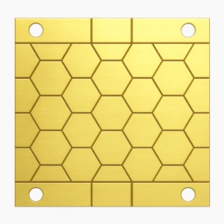
Direct Bonded Copper ceramic substrates for custom power and electronic substrate requirements.
DIRECT BONDED COPPERAMB陶瓷PCB
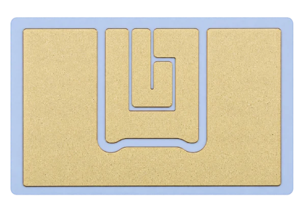
Active Metal Brazed ceramic substrates for high-current and high-reliability electronic applications.
ACTIVE METAL BRAZINGThick-Film Ceramic PCB
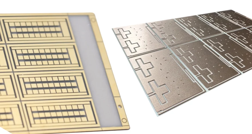
Thick-film ceramic substrates for specialized circuits, hybrid assemblies and custom electronic applications.
THICK FILMThin-Film Ceramic PCB
Thin-film ceramic substrates for fine-feature circuits and high-density electronic applications.
THIN FILMConfigure Your PCB
Choose the board construction, base material and fabrication requirements to get an instant indicative price range. Final pricing is confirmed after engineering review.
快速报价
准备好为您的下一个PCB项目报价了吗?
从原型制作到大批量生产,Highleap 为全球客户提供多层 PCB 制造、阻抗控制、快速工程审查和快速报价服务。