
Fabricación de placas IT-602G HDI para SSD y módulos de memoria
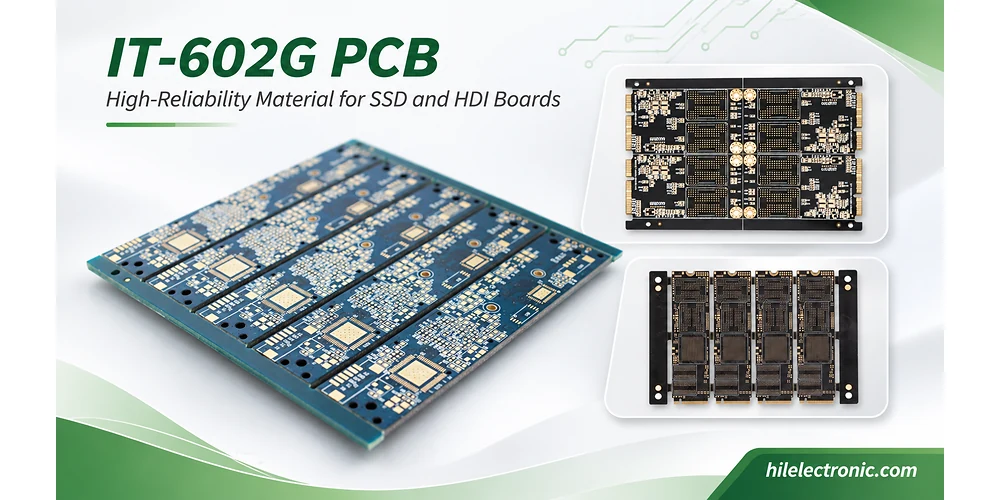
IT-602G PCB examples for HDI, SSD and memory-module applications.
An IT-602G PCB is typically considered when an HDI or memory-module design needs a halogen-free, high-Tg laminate with low dielectric loss and controlled Z-axis expansion. Those properties are relevant to sequential lamination and fine-pitch interconnects, but they do not remove the need to validate microvia geometry, dielectric thickness, copper balance and layer registration. Highleap Electronics fabricates and assembles boards specified with IT-602G; the manufacturing route is assessed against the released stack-up, drill data and assembly package.
ITEQ lists IT-602G for HDI, memory/SSD modules, server and telecom electronics. The supplier reports Tg of 210°C by TMA and a 10 GHz Dk near 3.5 with Df near 0.006, depending on specimen resin content. These material characteristics support the design; finished-board reliability also depends on dielectric geometry, via plating, registration and the assembly process.
IT-602G Material Properties in an HDI and High-Speed PCB Stack-Up
The main attraction of IT-602G is the combination of low Z-axis expansion and useful dielectric performance—not simply its high Tg. ITEQ’s current product sheet reports Tg of 210°C by TMA and 230°C by DMA, along with 1.1% cumulative Z-axis expansion from 50°C to 260°C. These are material-test figures. The stress on a plated via also depends on board thickness, hole diameter, barrel copper and the number of high-temperature excursions.
| Supplier-published parameter | IT-602G typical value | Why it matters during PCB manufacturing |
|---|---|---|
| Tg, TMA / DMA | 210 ° C / 230 ° C | Method must accompany a Tg comparison; the two readings are not interchangeable |
| Expansión del eje Z, 50–260 °C | 1.1% | Relevant to strain on plated-through-hole barrels and buried interconnects |
| Coeficiente de dilatación térmica X/Y, 40–125 °C | 9 / 9 ppm/°C | Helps plan registration around closely spaced features and large BGA arrays |
| Dk at 10 GHz, 55% / 70% resin samples | 3.85 / 3.47 | Actual pressed dielectric construction changes impedance calculations |
| Df at 10 GHz, 55% / 70% resin samples | 0.0060 / 0.0061 | Loss should be modeled using the appropriate sample and the entire channel |
| Decomposition temperature, 5% mass loss | 415 ° C | A thermal-stability metric, not an allowable continuous operating temperature |
The grade is listed with IT-602GTC copper-clad laminate and IT-602GBS prepreg designations. El glass-style and resin-volume choices that set the pressed dielectric matter as much as core selection: reinforcement style and resin fraction change dielectric spacing, resin availability beside etched copper, and the effective electrical properties. The approved construction should therefore be matched to a finished-thickness target rather than copied from a generic material table.
IT-602G is not an automatic substitute for every low-loss laminate. Its dielectric properties may suit a particular short or moderate channel, while a longer and faster link could require a lower-loss construction. That choice belongs inside the total interconnect budget, including copper foil, vias, connectors and package launches.
IT-602G PCB manufacturing for HDI and memory modules
An IT-602G PCB manufacturer needs more than the grade name on a fabrication drawing. The required core and prepreg styles, available dielectric thicknesses, lamination sequence and fine-hole geometry determine whether the specified multilayer construction is buildable. A memory-module or SSD controller PCB may have short interconnects yet still require tight BGA escape routing, closely spaced reference planes and reliable vias through several heat cycles.
For an OEM moving from concept toward engineering release, the fabrication package needs a controlled stack-up, a drill table that distinguishes mechanical and laser vias, impedance requirements and package-footprint data. These inputs allow the manufacturer to validate the HDI construction, via architecture and BGA escape strategy. The exact file set depends on the build-up sequence and should be finalized before production release.
Why Low Z-Axis Expansion Matters in Fine-Pitch HDI Interconnects
In-plane movement is not the same as finished-layer registration
The supplier lists X/Y CTE of 9/9 ppm/°C between 40°C and 125°C. As a purely illustrative expansion calculation, a 100 mm distance subject to a 100°C temperature change would change by approximately 100 × 9 × 10⁻⁶ × 100 = 0.09 mm if that simple constant-CTE model applied. This is not the residual registration error of a cooled manufactured PCB: artwork compensation, moisture movement, glass direction, tooling, cure shrinkage and press history also contribute. It does demonstrate why a tight capture-pad budget needs fabrication registration data, not just a low-CTE headline.
With a high-density memory module, via landing accuracy depends on several independent steps. Inner layers must align before pressing, panel movement must be accounted for, drill coordinates must reference the compensated panel, and copper features must retain adequate annular ring after all buildup stages. The laser microvia formation and sequential buildup operations therefore need separate registration and inspection controls rather than one overall tolerance.
In a conventional plated through-hole, the copper barrel and surrounding dielectric expand differently during soldering and service. The resin-rich laminate tends to move through the board thickness; barrel copper constrains that motion. Repeated strain can initiate fatigue at the knee of the hole, at internal-layer junctions or in weak plating sections. Low expansion reduces one stress contributor but cannot compensate for thin copper, resin smear or a poorly finished drill wall.
The effects become more demanding in HDI layouts. Blind vias, buried vias and sequential buildup layers add interfaces that must remain aligned through repeated pressing and imaging. The layer-pair definitions for a manufacturable HDI construction should make the lamination sequence explicit instead of hiding it inside the total layer count.
The registration budget should be defined against registration tolerances across successive lamination stages, because each press, drill and imaging cycle can add dimensional variation.
Mechanical interconnection and registration risks
- Via-to-pad geometry: smaller capture pads leave less tolerance for cumulative image shift, laser-drill alignment and plating variation. Critical microvia locations should be evaluated relative to the actual layer sequence.
- Microvías apiladas: interface integrity is influenced by how the microvia is filled, capped and plated, not just by the laminate’s Tg. Staggered structures may offer a different risk profile depending on routing density.
- Enrutamiento de escape BGA: a filled and capped via structure beneath fine-pitch BGA pads can shorten a dense escape path, but fill, copper-cap and planarization requirements must be defined on the fabrication drawing.
- Glass/resin distribution: fine traces across different weave regions can experience local effective-Dk variation; the PCB glass-weave effect is an electrical-layout issue as well as a laminate-construction issue.
Geometría meramente ilustrativa: a 1.6 mm board with a 0.20 mm finished through-hole has an 8:1 finished-hole thickness ratio. The drill diameter and plating requirements must still be chosen separately, and the example does not establish Highleap’s allowable aspect ratio. Hole-wall inspection and the actual thickness tolerance determine whether the structure is manufacturable.
Fine-pitch BGA and microvia reliability in an IT-602G HDI board
A fine-pitch BGA escape pattern may require via-in-pad or a small capture pad connected to a buried or staggered microvia. Those features introduce independent risks: laser-drill depth variation, incomplete target-pad preparation, voids in microvia metallization and misregistration between sequentially laminated layers. A material with low bulk Z-axis expansion does not eliminate an interface defect created during fabrication.
The selected drill diameter, capture-pad size and stacked-versus-staggered arrangement should follow microvia diameter, capture-pad and staggered-via design rules rather than a generic HDI label.
The qualification plan should identify the weakest interconnect geometry and the required evidence: finished capture-pad overlap, appropriate cross-sections, electrical continuity and any customer-defined thermal-stress or cycling tests. A broad statement that the material is suitable for HDI does not establish the reliability of a particular stacked-via design.
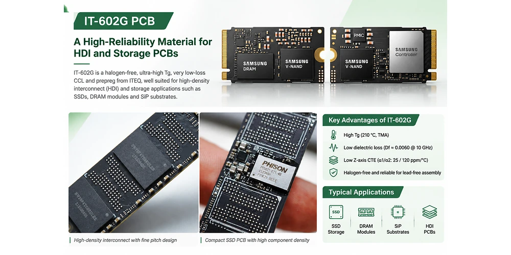
IT-602G storage and HDI application overview; construction values are reviewed against the supplier data and actual stack-up.
IT-602G Controlled-Impedance HDI Stack-Up and Lamination Planning
IT-602G is often described with Dk near 3.5 at 10 GHz, but the number is incomplete without a resin-content basis: supplier data distinguish 3.85 for a 55% resin specimen from 3.47 for a 70% specimen. The measurement of finished trace geometry against a specified impedance tolerance must therefore use the actual pressed dielectric thickness, finished trace width and etch profile.
The stack-up review should establish three linked dimensions
- Eléctrico: the intended impedance and insertion-loss targets, the signal’s relevant frequency range and the correct material-property basis.
- Física: pressed dielectric thickness, etched copper coverage, finished copper weight, foil profile and achievable trace-width tolerance.
- Proceso: how each lamination cycle changes thickness, registration, material movement and the location of buried features.
In practice, the choice between a nominal 0.10 mm and 0.13 mm dielectric cannot be made using Dk alone. It changes the required trace geometry for a target impedance and the amount of resin available to fill adjacent copper features. The relationship between copper pattern density and prepreg resin content deserves an explicit engineering check before the press cycle is released.
A dielectric-loss tangent is only one part of insertion loss. Conductor loss grows with frequency and depends on copper surface texture; transitions and discontinuities add further loss. If a channel fails its budget, replacing the laminate without first separating conductor, via and connector contributions may increase cost without solving the dominant cause.
FABRICACIÓN Y ENSAMBLAJE DE PCB
Planning an IT-602G HDI or memory-module PCB?
Highleap can discuss the HDI build-up, fine-pitch interconnects and PCB assembly scope for your IT-602G project.
Una primera consulta es sencilla. No complete Gerber or BOM package is needed to start. A short description of the HDI board and approximate quantity is enough; layer and drill details can follow when available for a firm quote.
Fabrication Sequence and Inspection Priorities for IT-602G Boards
What a representative HDI reliability coupon should expose
A useful coupon is deliberately built to reveal the design’s highest-risk interconnect—not merely a convenient hole in a generous copper field. If the production board contains blind vias on fine capture pads or a stacked transition, the qualification coupon may need to reproduce that feature’s copper thickness, dielectric interface and thermal history. Cross-sectioning can reveal separation at the base of a microvia, incomplete copper coverage or a crack through a plated interface. Electrical continuity testing is valuable, but a latent crack may not be evident until appropriate stress has been applied.
For stacked or staggered structures, microvia-interface evidence after thermal stress should be tied to the actual via architecture and the customer’s acceptance criteria.
Where a board includes repeated lamination cycles, the build sequence should also record when an already plated interconnect is exposed to another press cycle. The resin may be dimensionally stable while the copper interface accumulates strain. This is why material attributes and process qualification should be documented separately.
Multi-stage HDI manufacturing creates process risks that a finished-board Dk table cannot show. The process route should identify which internal layers are imaged and inspected before lamination, when blind/buried vias are drilled and plated, and how registration will be checked before subsequent buildup. The number of cycles is derived from the via architecture, not from a blanket statement about the material being suitable for HDI.
| Fase | mecanismo de fabricación | Evidence worth retaining |
|---|---|---|
| Inner-layer preparation | Copper distribution and etched-feature depth change resin demand | Approved layer artwork and press construction |
| Laminación y registro | Resin flow and thermal movement change dielectric thickness and alignment | Pressed cross-section, thickness and registration results |
| Drilling / desmear | Hole-wall damage or residual smear interrupts reliable copper adhesion | Drill-wall inspection and microsection evidence |
| Metallization / copper plating | Thin barrel sections or interface defects concentrate cyclic strain | Plating-thickness and microsection measurements |
| Final electrical verification | Dimensional drift shifts impedance even when the laminate grade is correct | Agreed impedance coupons and continuity/isolation tests |
Where fine holes cross resin/glass boundaries, hole-wall preparation before copper metallization is essential. Clean drilled walls and effective desmear support uniform metallization; representative microsections can distinguish local plating deficiency from substrate-related cracks or separation.
Qualification should reference the applicable customer drawing and the required IPC acceptance criteria. Material compliance to a base-material slash sheet is not the same thing as finished-board qualification to IPC-6012 or visual acceptability to IPC-A-600. Where thermal cycling is important, the test coupon should represent the actual via architecture and critical material interfaces.
SSD and Memory-Module PCB Assembly with IT-602G
Avoid losing the board-level benefit during assembly transfer
The fabrication drawing and assembly drawing should refer to the same revision and stack-up. If assembly engineering changes a BGA footprint or solder-mask opening to improve paste release, that change can affect via-capture geometry, copper balance or the routing strategy on a fine HDI layer. Conversely, changing a via fill or surface finish after an SMT program has been validated may alter solder-joint formation. The manufacturing review should identify these cross-disciplinary changes before releasing production artwork.
A first build should distinguish board-level open/short defects, solder-joint defects and functional failures. The evidence needed for each is different: electrical test and microsection for the bare board; imaging and assembly inspection for the solder joints; and product-specific functional testing for the complete module. None is a substitute for the others.
A high-density bare board must also survive the selected soldering profile. For memory modules, SSD boards and fine-pitch packages, surface finish, BGA escape geometry, solder-mask alignment and board warpage interact during assembly. The BGA soldering and inspection requirements for dense interconnect boards should be reviewed while the stack-up is finalized, not after laminate procurement.
An electrically sound via can be damaged during excessive localized rework; a flat bare board can warp when populated asymmetrically. Moisture handling, stencil design, component placement, reflow limits and the appropriate inspection method have to be aligned to the actual bill of materials and board construction. Where hidden joints are involved, inspection should be capable of distinguishing solder voiding or bridging from an underlying bare-board defect.
During detailed engineering review, Highleap can assess IT-602G material availability, stack-up construction, drilling and plating requirements, agreed PCB testing and the requested assembly scope. Gerber or ODB++ data, drill information, stack-up and assembly details are reviewed according to the board’s complexity and the manufacturing steps involved.
What should an SSD controller PCB assembly quote include?
Before an SSD controller PCB or memory-module assembly enters production, the BOM and component revisions, BGA pitch, placement data, assembly drawing, solder-joint requirements, test coverage and approved bare-board finish must be reconciled. These are production-planning details, not prerequisites for an initial inquiry. If via fill, solder-mask openings or pad dimensions are still being finalized, they can be resolved during the engineering handoff before SMT programming begins. Highleap can assess the bare-board and populated assembly as one coordinated PCB/PCBA scope.

Sobre la autora
shirley leung
Gerente de productos PCB/PCBA e ingeniero técnico de ventas
Shirley cuenta con 5 años de experiencia práctica en fabricación y ensamblaje de PCB. Su experiencia abarca placas multicapa complejas, estructuras HDI, suministro de componentes llave en mano, ensamblaje SMT, pruebas e integración completa de sistemas.
Como asesora técnica y especialista en ventas, apoya a los clientes con orientación DFM, optimización de costos y planificación de producción, ayudando a que los proyectos avancen de manera eficiente desde el diseño hasta la producción en masa con una calidad constante y una entrega a tiempo.

Mensajes recomendados
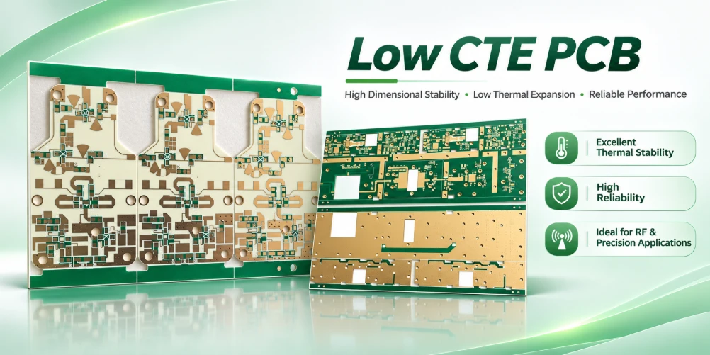
Fabricación de placas de circuito impreso (PCB) con Arlon 45NK de bajo coeficiente de dilatación térmica (CTE) en China
Ilustración de fabricación de PCB. Confirme lo especificado...
Servicios de fabricación de PCB de Arlon 85HP en China
Ilustración de fabricación de PCB. Confirme lo especificado...
Fabricación de PCB Arlon 86HP HDI
Ilustración de fabricación de PCB. Confirme lo especificado...
Fabricación y ensamblaje de PCB de alta Tg KB-6169GT
HIGHLEAP ELECTRONICS / KB-6169GT / Fabricación de PCB de alta temperatura de transición vítrea...
Cómo obtener una cotización para PCB
Realicemos un análisis DFM/DFA y le enviaremos un informe. Puede subir sus archivos de forma segura a través de nuestro sitio web. Necesitamos la siguiente información para poder ofrecerle un presupuesto:
-
- Gerber, ODB++ o .pcb, especificación.
- Lista de materiales si necesita ensamblaje
- Cantidad
- Convertir el tiempo
Además de la fabricación de PCB, ofrecemos una amplia gama de servicios electrónicos, incluyendo diseño de PCB, PCBA y soluciones llave en mano. Ya sea que necesite ayuda con el prototipado, la verificación del diseño, el suministro de componentes o la producción en masa, le brindamos soporte integral para garantizar el éxito de su proyecto.
Para servicios de PCBA, proporcione su lista de materiales (BOM) e instrucciones de montaje específicas. También ofrecemos análisis DFM/DFA para optimizar la fabricación y el montaje de sus diseños, garantizando así un proceso de producción sin problemas.