
HIGHLEAP ELECTRONICS / KB-6165LE / MULTILAYER PCB PRODUCTION
Fabricación y ensamblaje de PCB multicapa KB-6165LE
Looking for a manufacturer for your KB-6165LE multilayer PCB? Highleap Electronics works from your existing board files and approved material specification. We quote new builds, pilot runs and repeat orders, with optional component sourcing and assembly. You can start with the files you already have; we will identify any missing details.
Envíenos sus archivos de PCB, los requisitos de material y la cantidad para obtener un presupuesto de fabricación.
KB-6165LE PCB Manufacturing for New and Existing Designs
If KB-6165LE is already written into your PCB fabrication drawing, your immediate need is likely a manufacturer that can reproduce the approved board—not an explanation of why the engineer selected that material. Highleap Electronics quotes custom KB-6165LE multilayer PCBs from existing manufacturing data and can support the next pilot lot, production order or supplier transfer.
You can send the Gerber or ODB++ package you received from engineering, together with the quantity and desired delivery window. If the fabrication notes or drawings are included, we use them to identify the specified layer sequence, thickness, finishes and acceptance requirements. Where something is unclear, we raise a focused engineering question instead of asking purchasing to recreate the complete stackup.
Nuestra visión más amplia Servicio de fabricación de PCB multicapa covers conventional rigid multilayer production and more complex constructions. With KB-6165LE, we first confirm the named material and the actual multilayer build can be sourced and manufactured as requested.
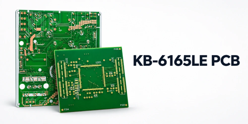
KB-6165LE Multilayer Production
The critical point for a KB-6165LE PCB order is consistent execution of the approved multilayer construction. Material designation, layer thickness, copper, hole geometry and surface finish need to match the released design. Highleap reviews those details together so a board does not appear acceptable on a quotation while important manufacturing assumptions remain unresolved.
Layer buildup and core/prepreg consistency
A multi-layer PCB is purchased as a finished, dimensioned assembly of conductive and insulating layers. For a specified KB-6165LE construction, we review the existing layer map, board thickness and dielectric requirements. We can identify the proposed core/prepreg combination for manufacturing approval where the submitted package does not already lock it down.
This matters particularly when an OEM has qualified a specific board revision and expects the next supplier to reproduce it. A higher or lower nominal Tg is not a free pass to substitute another laminate. Kingboard identifies KB-6165LE as a mid-Tg, anti-CAF material with low Z-axis expansion. We use that identification to check the requested purchase specification—not to promise that a finished PCB has passed the customer’s thermal cycling tests.
Drill, plating and through-hole features
A thicker board with many plated through-holes, small finished holes or dense connector areas can require closer production attention than a simpler board made from the same laminate. Highleap reviews drilled-hole information against board thickness, copper plating, finished dimensions and the specified inspection level. This is relevant to conventional PTHs, press-fit holes and other customer-defined interfaces.
Where the drawing calls for blind/buried vias, filled vias or a special via structure, we evaluate the build sequence rather than treating all holes as interchangeable. Highleap lists advanced via options within its Capacidades de PCB rígidas; suitability for this KB-6165LE stackup is confirmed during the review.
Controlled impedance and copper configuration
If your board includes impedance-controlled connections, we can quote the defined stackup and coupon requirements. The manufacturing discussion is about agreed finished geometry and test evidence, not inventing a new electrical target. Copper weight, conductor density and layer balance also affect yield and cost, especially when the board is thick or tightly routed.
For a new design, engineering may be willing to review a stackup suggestion. For a supplier-transfer job, changes to the approved construction should go back to the customer’s design authority before release.
Surface finish, outline and final inspection
A KB-6165LE PCB may call for ENIG, OSP, HASL, immersion tin or another drawing-specified finish. A press-fit connector design may also need tight hole and outline tolerances; an edge-contact product may require a separate gold-plating step. These are real manufacturing choices and are included in the quote where applicable.
Nuestros PCB surface finish service describes available finishing routes. The exact combination of material, finish and special processes is reviewed for each design rather than assumed to be available in every configuration.
| Part of the released design | What Highleap checks before confirming production |
|---|---|
| KB-6165LE laminate and layer buildup | Named material, board thickness, dielectric construction and sourcing |
| Finished holes and plated features | Drilling method, hole size, plating, press-fit features where specified |
| Copper and electrical requirements | Trace geometry, finished copper, controlled-impedance requirements |
| Surface finish and mechanical outline | ENIG/OSP/HASL or specified finish, routed profile, slots and tolerance |
| Agreed quality evidence | Electrical test, critical measurements and any additional records ordered |
Moving a Qualified Board to Highleap
A supplier transfer should make it easier for purchasing to secure boards, not force engineers to redesign an approved product. If you are changing PCB suppliers, send the latest manufacturing package, current board revision and any existing purchase or quality notes. If you have an approved material list or a previous build specification, include it if available.
Highleap can compare the received package with the required production route and identify discrepancies before the first lot. We can also discuss first-article inspection, a pilot quantity and what evidence you want to receive with the shipment. The agreed baseline then supports later repeat orders.
This is particularly useful when the board will be assembled elsewhere. The new bare board needs to preserve the fit, footprint and finish expected by the established assembly process. If the supplier transition also includes assembled boards, our Soporte para la transferencia de producción de ensamblaje de PCB covers that broader handover.
Cost, Surface Finish and Lead Time for KB-6165LE PCBs
The KB-6165LE material name does not determine the finished PCB price. We price the actual board: dimensions and panel yield, layer count and thickness, copper, hole complexity, required finish, any special lamination or via work, inspection scope and order quantity.
Surface finish and special processing are not minor details. An ENIG finish may have a different cost than OSP or HASL. Resin-filled vias, via-in-pad, blind/buried vias, tight press-fit holes, backdrilling or demanding impedance testing can add process steps when the drawing requires them. These features also influence the achievable production schedule.
Material availability is checked before committing to delivery. If the grade or construction must be specially sourced, we will account for that in the quotation rather than advertise an unrealistic standard lead time. For a recurring program, estimated order frequency and annual demand can help planning, but you can still request a one-off quote without a yearly forecast.
An OEM with a different design calling for standard KB-6165F PCB manufacturing can ask for a separate quote. The two materials should not be interchanged in an already-approved board without authorization.
Bare Boards or PCB Assembly from One Supplier
Highleap can ship KB-6165LE bare boards or quote component procurement, SMT, through-hole assembly and agreed testing. This lets an OEM choose whether to keep its current assembler or combine board manufacturing and PCBA under one purchase order.
Nuestra publicación Servicios de montaje de PCB include AOI, X-ray inspection for applicable packages and functional testing when a test procedure is provided. If the project involves double-sided reflow, large connectors or special assembly support, we coordinate the process with the approved board construction before release.
The same commercial principle applies to PCBA: provide the BOM and placement or assembly data you already have. Highleap reviews it and follows up about omissions or conflicts; purchasing should not have to specify solder profiles and component handling details from scratch.
Solicite un presupuesto para la placa de circuito impreso KB-6165LE.
Send your existing fabrication files and order quantity through our página de cotización rápida. Add a target delivery date and, if you need assembly, a BOM. Highleap will check the KB-6165LE callout, finished-board processing and any special quality requirements, then respond with a quote or specific clarification questions.
Whether you are buying a first prototype, transferring an approved multilayer board or planning repeat production, the starting point is the same: your current design files are enough to begin the manufacturing review.

Mensajes recomendados
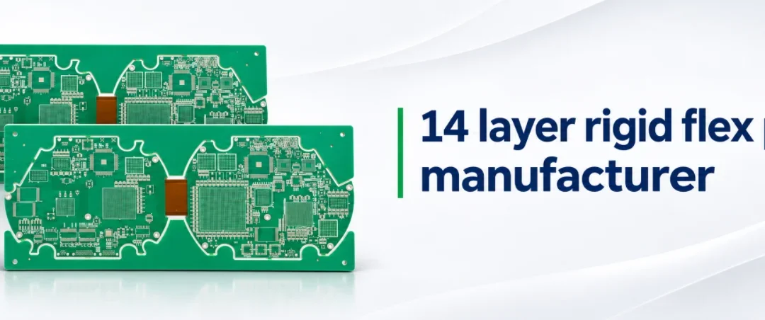
Fabricante chino de placas de circuito impreso rígido-flexibles de 14 capas para la fabricación de productos OEM personalizados.
ZONAS RÍGIDAS + FLEXIBLES · HIGHLEAPHighleap Electronics...

Fabricante chino de placas de circuito impreso de 14 capas con panel posterior para ensamblajes de ajuste a presión.
HIGHLEAP ELECTRONICS / PLACAS TRASERAS / PRESIÓN...
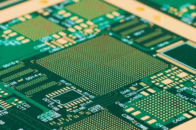
Fabricante chino de placas de circuito impreso HDI de 14 capas para placas con microvías personalizadas.
HIGHLEAP ELECTRONICS / MICROVIAS / SECUENCIAL...
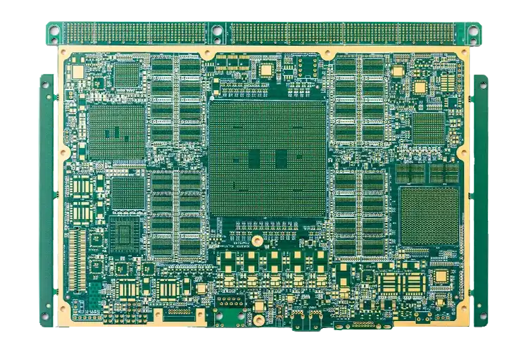
Fabricante de PCB de 14 capas en China
PCB RÍGIDO MULTICAPA PERSONALIZADO Highleap Electronics...
Cómo obtener una cotización para PCB
Realicemos un análisis DFM/DFA y le enviaremos un informe. Puede subir sus archivos de forma segura a través de nuestro sitio web. Necesitamos la siguiente información para poder ofrecerle un presupuesto:
-
- Gerber, ODB++ o .pcb, especificación.
- Lista de materiales si necesita ensamblaje
- Cantidad
- Convertir el tiempo
Además de la fabricación de PCB, ofrecemos una amplia gama de servicios electrónicos, incluyendo diseño de PCB, PCBA y soluciones llave en mano. Ya sea que necesite ayuda con el prototipado, la verificación del diseño, el suministro de componentes o la producción en masa, le brindamos soporte integral para garantizar el éxito de su proyecto.
Para servicios de PCBA, proporcione su lista de materiales (BOM) e instrucciones de montaje específicas. También ofrecemos análisis DFM/DFA para optimizar la fabricación y el montaje de sus diseños, garantizando así un proceso de producción sin problemas.