
Fabricación de placas de circuito impreso para mini PC: placas base compactas de alta densidad.
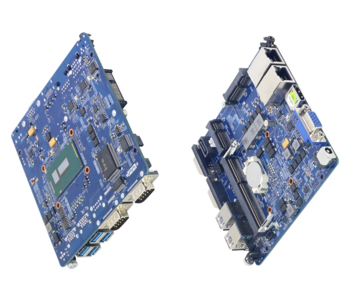
Tabla de contenidos.
- Defina la arquitectura compacta antes de seleccionar la construcción de la PCB.
- Opciones de HDI, apilamiento e impedancia para placas de mini PC de alta densidad
- Ensamblaje de BGA y PCBA de doble cara en un área de placa pequeña
- Convierta el diseño térmico en instrucciones de fabricación controladas.
- E/S de borde, antenas y ajuste de la carcasa
- Lista de materiales (BOM), referencias de producto (SKU), costes y escalado de producción para plataformas informáticas compactas.
- Pruebas funcionales para placas de circuito impreso de mini PC con y sin ventilador.
- Consideraciones sobre el abastecimiento global para placas de circuito impreso compactas y para computación perimetral.
- Enviar a Highleap los datos necesarios para una revisión de la fabricación de mini PC.
Un mini PC concentra el procesador, la memoria, el almacenamiento, la conversión de energía, la conectividad inalámbrica y las E/S externas en una placa base compacta. El desafío de fabricación no reside únicamente en la miniaturización, sino en preservar el rendimiento de la señal, la energía, la gestión térmica y las características mecánicas cuando el espacio para el cableado, la separación entre componentes y el espacio libre en la carcasa son limitados.
Highleap Electronics ofrece soporte para proyectos de placas base de mini PC propiedad del cliente, desde la fabricación de PCB hasta el ensamblaje de PCBA, la selección de componentes homologados, la programación y las pruebas funcionales definidas por el cliente. El diseño final determina si la placa utiliza una estructura multicapa convencional, HDI, vías ciegas, microvías u otras características de densidad. No existe un número de capas o una arquitectura de vías que sea la correcta para todos los mini ordenadores.
Las placas base compactas x86, las placas para mini PC sin ventilador, los miniordenadores integrados y las plataformas informáticas de formato pequeño pueden presentar problemas de fabricación similares, a pesar de utilizar procesadores, tipos de memoria, almacenamiento, redes y sistemas térmicos muy diferentes. Por lo tanto, el proceso de fabricación debe basarse en la densidad de paquetes, el conjunto de interfaces y el diseño del chasis.
1. Defina la arquitectura compacta antes de seleccionar la construcción de la PCB.
Las decisiones sobre la densidad comienzan con la ubicación y la arquitectura de interconexión. El procesador o el SoC, la ubicación de la memoria, el almacenamiento M.2, el módulo Wi-Fi, las etapas de potencia, los controladores Ethernet y los conectores laterales compiten por un espacio limitado para el enrutamiento y el área de componentes. Si estas relaciones no son estables, seleccionar una estructura de vías costosa demasiado pronto puede generar una complejidad de fabricación innecesaria para el proyecto.
Capa / Vía Estrategia
Highleap puede revisar la placa liberada mediante un análisis DFM antes de la fabricación. Los datos más útiles son el paquete Gerber u ODB++, la configuración de capas, la tabla de perforación, los requisitos de impedancia, la lista de materiales (BOM), la lista de componentes (CPL) y el plano mecánico que muestra las paredes de la carcasa, las aberturas de los conectores, las zonas de disipación de calor y los puntos de montaje.
Disciplina de fabricación
El objetivo de producción debe ser la construcción de placa más sencilla que cumpla con el diseño eléctrico y mecánico aprobado, con el margen de proceso adecuado. Un tamaño compacto no justifica automáticamente la HDI, mientras que una alta densidad de conexiones BGA o un contorno de placa restringido pueden convertirla en la solución práctica.
2. Opciones de HDI, apilamiento e impedancia para placas de mini PC de alta densidad
Cuando la densidad de enrutamiento requiere vías ciegas, microvías o laminación secuencial, la configuración de capas debe presentarse como una estructura de fabricación en lugar de un simple esquema visual. La profundidad de las microvías, las almohadillas de captura, los requisitos de vías rellenas o tapadas, el grosor del cobre, la construcción dieléctrica y la secuencia de laminación influyen en el rendimiento y el coste.
Controles clave de fabricación
- Capa / Vía Estrategia: Los recursos de fabricación de PCB HDI de Highleap son relevantes cuando la placa base compacta realmente necesita esas características. Para diseños que permiten el enrutamiento con vías pasantes, una construcción multicapa convencional puede ser más económica y más fácil de transferir a la producción en serie.
- Disciplina de fabricación: Las interfaces rápidas como DDR, PCIe, USB, Ethernet y las conexiones de pantalla deben seguir la configuración de apilamiento y la geometría de impedancia definidas por el cliente. El control de fabricación debe incluir la continuidad del plano de referencia, las transiciones de vía y la verificación de impedancia requerida, en lugar de basarse en una etiqueta de material genérica. El sistema de materiales debe seleccionarse en función de los requisitos reales de señal, térmicos, de espesor y de fiabilidad de la placa.
3. Ensamblaje de BGA y PCBA de doble cara en un área de placa pequeña
Las placas de circuito impreso para mini PC suelen colocar componentes en ambos lados para optimizar el espacio disponible. Esto aumenta la complejidad de la planificación del proceso, ya que la combinación de componentes del primer lado, el reflujo del segundo lado, la masa del encapsulado, la estrategia de plantillas y las herramientas de soporte pueden interactuar. Los conectores BGA, QFN, LGA y de paso fino, de alta densidad, también reducen la tolerancia a errores de impresión o colocación.
Highleap puede combinar el ensamblaje de PCB SMT con controles de ensamblaje BGA específicos cuando la combinación de encapsulados lo requiera. El plan de construcción debe especificar qué lado se ensambla primero, qué componentes necesitan soporte especial, qué uniones ocultas se inspeccionan mediante rayos X y qué conectores requieren una operación independiente.
Control de montaje
- Revise las aberturas de la plantilla alrededor de los circuitos integrados de paso fino y los encapsulados de almohadillas térmicas.
- Controle los componentes sensibles a la humedad de acuerdo con los requisitos de manipulación aprobados.
- Utilice la inspección de la primera pieza para verificar la densidad de las opciones y la polaridad antes de la colocación del lote.
- Compruebe que los componentes altos y las zonas de exclusión inferiores cumplan con las limitaciones de la fijación y del chasis.
- Limite los trabajos de retrabajo innecesarios en torno a procesadores costosos, dispositivos de memoria y conectores de paso fino.
Highleap Electronics • Fabricación de PCB y ensamblaje de PCBA
Solicitar una revisión del proceso de fabricación de PCB para mini PC
Envíe sus archivos Gerber u ODB++, la lista de materiales (BOM), los datos de ensamblaje y la cantidad. Highleap revisará la fabricación de la placa de circuito impreso, el abastecimiento, el ensamblaje, la programación y el alcance de las pruebas para garantizar un montaje controlado.
Solicitar presupuesto para PCB y PCBA → Analizar requisitos de fabricación →
✓ Revisión DFM y DFA ✓ Prototipo para producción en serie ✓ Fabricación y ensamblaje de PCB
4. Transforme el diseño térmico en instrucciones de fabricación controladas.
Los sistemas de formato compacto disponen de menos espacio para la circulación del aire y la disipación del calor, por lo que el rendimiento térmico depende en gran medida del diseño completo del sistema. El fabricante de PCB no puede crear una solución térmica adecuada modificando el cobre o añadiendo vías sin la aprobación del diseño. En su lugar, los planos de PCB y de montaje deben identificar las zonas de vías térmicas, las áreas de cobre, los puntos de montaje del disipador, las zonas de interfaz térmica y cualquier componente cuya altura o ubicación sea crítica para el sistema de refrigeración.
Interfaces térmicas
En la línea de ensamblaje de placas de circuito impreso (PCBA), las superficies de interfaz térmica deben protegerse de la contaminación y los daños mecánicos. Si se le solicita a Highleap que instale un disipador de calor, un ventilador, una almohadilla térmica u otro componente térmico aprobado, las instrucciones de trabajo deben especificar el número de pieza, la ubicación, el método de fijación y el punto de inspección.
control de fábrica
Los proyectos de mini PC sin ventilador requieren especial atención, ya que la carcasa puede formar parte de la ruta de disipación de calor. Una prueba funcional a nivel de placa no puede garantizar que el sistema final se mantenga dentro de los límites de temperatura de los componentes bajo cualquier carga de trabajo. Dicha validación corresponde al plan completo de cualificación térmica y del sistema del cliente.
5. E/S de borde, antenas y ajuste de la carcasa
Las placas de mini PC suelen colocar los conectores USB, Ethernet, HDMI/DisplayPort, de audio, de alimentación y otros directamente en el borde de la placa base. Pequeños errores de alineación pueden hacerse visibles inmediatamente cuando la placa de circuito impreso se instala en una carcasa mecanizada o moldeada con gran precisión.
Restricciones físicas
El plano de montaje debe identificar la ubicación de los conectores y los puntos de referencia mecánicos, mientras que el plano de la carcasa debe definir las aberturas, los separadores y las zonas de interferencia. Los diseños inalámbricos también requieren conectores de antena, rutas de cableado y áreas de exclusión aprobados. Si el producto utiliza una placa de E/S frontal o secundaria independiente conectada mediante FPC o cable, dicha interfaz debe considerarse parte del conjunto de electrónica controlada, en lugar de un accesorio de integración informal.
Control de fabricación
| Control mecanico | Pregunta de producción |
|---|---|
| Conectores laterales | ¿El conector insertado coincide con la abertura del chasis liberada y la dirección de inserción? |
| Módulos M.2 e inalámbricos | ¿Hay espacio suficiente para el módulo, el hardware de retención y el enrutamiento de la antena/cable? |
| Disipador de calor o difusor de calor | ¿Los puntos de montaje, las zonas de exclusión y las alturas de los componentes coinciden con la configuración mecánica aprobada? |
| Placa hija o FPC | ¿Están definidas la orientación del conector, la longitud del cable y la dirección de la curvatura? |
| Orificios de montaje y separadores | ¿Se puede fijar la placa sin doblarla ni sobrecargar los componentes cercanos? |
6. Lista de materiales, referencias, costes y escalado de producción para plataformas informáticas compactas
Los programas informáticos compactos suelen crear múltiples configuraciones a partir de una misma placa base: distintas opciones de memoria o almacenamiento, módulos Wi-Fi, controladores Ethernet, módulos celulares o funciones de entrada/salida. Una placa de circuito impreso compartida puede ser eficiente, pero solo si la fábrica recibe una matriz de variantes clara.
Integridad de la lista de materiales
Highleap puede incluir el suministro de componentes con alternativas controladas por el cliente. Las piezas sensibles a la plataforma deben estar bloqueadas o sujetas a aprobación, mientras que los componentes pasivos verdaderamente intercambiables pueden seguir reglas de suministro acordadas. La lista de materiales debe identificar cualquier módulo suministrado por el cliente y si Highleap o el cliente se encargan de su instalación y prueba tras el envío.
SKU / Riesgo del ciclo de vida
Para programas OEM de larga duración, el control del firmware y las referencias de producto (SKU) deben estar vinculados a la revisión del hardware. Una orden de producción no debe depender de que los operarios interpreten nombres de productos como «versión sin ventilador» o «versión con doble LAN» sin una lista de materiales (BOM) y un perfil de prueba controlados.
Escalado de la producción y control comercial
El coste de las placas de circuitos impresos mini aumenta cuando la densidad requiere más capas, laminación secuencial, microvías ciegas, tolerancias más estrictas o una inspección más exigente. El coste de ensamblaje puede incrementarse con la colocación a doble cara, los encapsulados BGA, los conectores de paso fino, las operaciones de E/S manuales, los módulos suministrados por el cliente, la programación y una amplia cobertura de pruebas funcionales.
Prototipo
El diseño del prototipo debe identificar qué complejidad es estructuralmente necesaria y cuál puede simplificarse. Si la placa puede pasar de una estructura HDI a una construcción multicapa convencional sin alterar su rendimiento eléctrico o mecánico, se trata de una decisión que implica un ahorro de costes significativo. Si se requiere HDI para evitar el procesador y cumplir con las dimensiones de la carcasa, eliminarlo solo traslada el riesgo al enrutamiento o la fiabilidad.
Piloto / NPI
Antes de la producción en serie, defina la configuración aceptada, incluyendo la estructura, las reglas de la lista de materiales, la imagen de programación, el método de prueba y las instrucciones de ensamblaje mecánico. Esta base de producción es más importante que el precio de un prototipo único.
7. Pruebas funcionales para placas de circuito impreso de mini PC con y sin ventilador
Las pruebas de las placas de circuito impreso de los mini PC deben verificar las funciones críticas para la fabricación antes de que la placa se integre en un chasis compacto. Según el diseño, la ruta de prueba puede incluir comprobaciones de rieles/cortocircuitos, identificación del firmware, detección de memoria, interfaces de almacenamiento, enlace Ethernet, puertos USB/pantalla seleccionados, salidas de control de ventiladores y comprobaciones inalámbricas o de periféricos definidas por el cliente.
Funciones a nivel de sistema
Highleap puede realizar pruebas funcionales de PCB según los procedimientos y límites de aceptación proporcionados por el cliente. Si se requiere validación térmica, rendimiento acústico o estabilidad bajo cargas de trabajo prolongadas, estas pruebas deben definirse por separado, ya que pueden depender de la carcasa final, el sistema de refrigeración, la carga de software y las condiciones ambientales.
8. Consideraciones sobre el abastecimiento global para placas de circuito impreso compactas y para computación de borde.
El hardware de los mini PC se utiliza en más de una categoría de productos: sistemas de oficina compactos, nodos de computación integrados, pasarelas de borde y pequeños ordenadores industriales pueden usar una placa base de alta densidad, pero sus requisitos de E/S, térmicos y de ciclo de vida difieren. Esto hace que la geografía sea útil como contexto de adquisición, no como razón para obligar a que todos los mini PC se ajusten a una única configuración.
Estados Unidos y Canadá: Programas de hardware desde el prototipo hasta la producción a gran escala
Para los equipos que evalúan a un fabricante de PCB para mini PC en China , la solicitud de cotización debe mostrar los factores determinantes de la densidad: encapsulado del procesador o SoC, arquitectura de memoria, almacenamiento M.2, Ethernet, salidas de vídeo, módulos inalámbricos, entrada de alimentación y límites de la carcasa. De esta forma, el proveedor puede determinar si la fabricación multicapa convencional es suficiente o si el diseño publicado requiere características HDI.
Alemania, Países Bajos y Reino Unido: Integración de la computación industrial y de borde
Los proyectos europeos de informática compacta suelen integrarse en máquinas más grandes, quioscos, plataformas de automatización o dispositivos de red. Para un proveedor de ensamblaje de placas de circuito impreso para mini PC , el acceso a los conectores, la referencia de montaje, la ubicación de la interfaz térmica, la configuración con o sin ventilador, el firmware operativo y las decisiones sobre la lista de materiales de larga duración pueden ser tan importantes como el tamaño de la placa.
Japón, Corea del Sur y Singapur: Electrónica de alta densidad y coordinación de la cadena de suministro
Los equipos de ingeniería en estos mercados tecnológicos de Asia-Pacífico pueden gestionar ecosistemas avanzados de componentes, empaquetado e integración de sistemas. Al comparar un proveedor de PCB para placas base de ordenadores compactos , algunos datos útiles incluyen la fabricación con apilamiento controlado, el control del proceso BGA, el ensamblaje de doble cara, el análisis por rayos X cuando se especifica, el abastecimiento aprobado y una ruta de prueba funcional repetible.
El modelo de fabricación internacional de Highleap permite la producción de prototipos, nuevos productos y producción en serie. Incluya el país de destino y la previsión en el archivo técnico para que el embalaje, la logística, el suministro de materiales y las expectativas de producción recurrente sean visibles durante la cotización.
9. Enviar a Highleap los datos necesarios para una revisión de la fabricación de mini PC.
Para obtener un presupuesto de PCB/PCBA para mini PC, proporcione los archivos Gerber u ODB++, información sobre la configuración de apilamiento y perforación, la lista de materiales (BOM), datos de colocación de componentes, plano de ensamblaje, cantidad y estado de revisión. Incluya el plano mecánico, la información de ensamblaje térmico y el procedimiento de firmware/prueba cuando estas operaciones formen parte del alcance de la fabricación.
Evaluación de fábrica
Highleap puede revisar el paquete para la fabricación de PCB, la viabilidad de HDI cuando sea necesario, el ensamblaje de PCBA, el abastecimiento, la inspección y las pruebas definidas por el cliente. Envíe los archivos a través de la página de cotización de ensamblaje de PCB.

Mensajes recomendados

Fabricación de PCB con filtro TMM4
La fabricación de la placa de circuito impreso del filtro TMM4 está controlada por...

Fabricación de PCB TMM3 para módulos de RF
La fabricación de PCB TMM3 es más útil donde el módulo de RF...

Fabricación de PCB TMM6
La fabricación de TMM6 es la página de control de procesos para un sistema de fabricación de mediados de siglo...

Fabricación de PCB TMM10 para diseños de RF compactos
Tabla de contenido Cómo TMM10 reduce el tamaño de las estructuras de RF TMM10 vs...
Cómo obtener una cotización para PCB
Realizaremos un análisis DFM/DFA y le enviaremos un informe. Puede subir sus archivos de forma segura a través de nuestro sitio web. Para poder ofrecerle un presupuesto, necesitamos la siguiente información:
-
- Gerber, ODB++ o .pcb, especificación.
- Lista de materiales si necesita ensamblaje
- Cantidad
- Convertir el tiempo
Para servicios de PCBA, proporcione su lista de materiales (BOM) e instrucciones de montaje específicas. También ofrecemos análisis DFM/DFA para optimizar la fabricación y el montaje de sus diseños, garantizando así un proceso de producción sin problemas.