
ITEQ IT-170GRA2 -piirilevy: Yhteensopiva suunnittelu ja signaalihäviöiden testaus
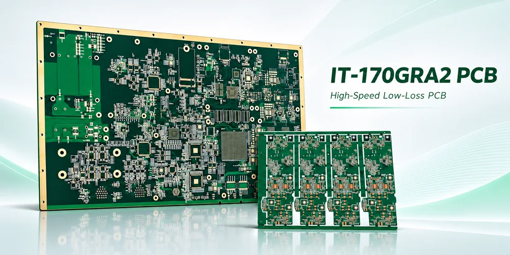
Illustration of high-speed PCB layouts.
ITEQ IT-170GRA2 is a halogen-free, high-Tg epoxy laminate and prepreg for lower-loss multilayer PCBs. ITEQ reports a dielectric constant (Dk) of 3.8 and a dissipation factor (Df) of 0.0080 at 10 GHz on a 50% resin-content specimen. That is a useful starting point for selecting a server, storage, networking or backplane stack-up. The decision to use it belongs to the channel loss budget.
Give the PCB its share of the channel loss budget
Start with a frequency-dependent limit and define the electrical reference planes. If the limit is specified from transmitter package to receiver package, reserve margin for the packages, connectors, launches, via transitions and fabrication variation before assigning the remaining loss to routed board traces. For a simple NRZ link, half the bit rate is the Nyquist frequency; for a multilevel link, use the symbol rate and the applicable specification. A single Nyquist checkpoint is useful for screening, but a production mask may cover a band and include return loss, crosstalk or mode conversion as separate requirements.
A first-pass loss allocation can add estimated positive loss contributions in decibels when the sections are well matched. Then cascade the actual transition and line models or measure the representative channel. Reflections can make the insertion-loss curve ripple, so the arithmetic budget is not a substitute for the cascaded result. Decide early which transitions belong to the board supplier’s test and which must wait until connectors or components are populated.
Compare the longest routed layer segments first. Where the dominant loss is in a long uniform trace, a lower-Df construction and a suitable foil may buy more margin. A short path with a deep plated via stub or a poorly referenced connector launch may benefit more from a layout change. In that second case, putting IT-170GRA2 into the same artwork may leave the main loss mechanism in place.
IT-170GRA2 Dk and Df by frequency
Käyttää IT-170GRA2TC as the laminate designation and IT-170GRA2BS as the prepreg designation when reconciling the drawing with ITEQ’s data. ITEQ lists Tg as 175°C by DSC and 170°C by TMA. Neither value replaces component and solder-paste limits for assembly.
| Taajuus | Dk | Df | IPC-TM-650 method |
|---|---|---|---|
| 1 GHz | 4.0 | 0.0060 | 2.5.5.9 |
| 2 GHz | 3.9 | 0.0063 | 2.5.5.13 |
| 5 GHz | 3.9 | 0.0075 | 2.5.5.13 |
| 10 GHz | 3.8 | 0.0080 | 2.5.5.13 |
Lähde: ITEQ IT-170GRA2 datasheet, Rev. 1.0-26. The frequency points report test results; the table does not define a frequency limit for a product or a guaranteed loss per unit length.
How does it compare with IT-170GT? ITEQ reports 0.0095 Df at 10 GHz and 55% resin content for IT-170GT. The listed values point toward IT-170GRA2 when dielectric loss is the primary concern. They come from different resin contents, so applying the percentage difference directly to a finished channel would be misleading. Recalculate impedance and insertion loss for the proposed glass, pressed thickness and foil before approving a substitution.
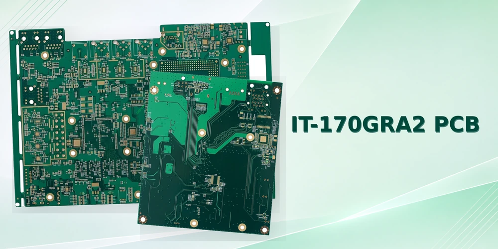
High-speed routing illustration. Evaluate channel loss on the specified stack-up and transitions.
Control the fabrication variables in the field model
Specify the copper surface that faces the dielectric
The smoothness of a foil label alone does not define conductor loss. The bonding treatment and roughness on the relevant copper surface change the current path when skin effect becomes significant. ITEQ’s sheet reports peel strength for a 35 µm low-profile foil reference; peel strength cannot be converted to the roughness parameters needed by a channel solver. Freeze the foil designation and treatment for the signal layer and its reference as applicable, and request roughness information compatible with the solver model. A change in Piirilevyn kuparin karheus can move the loss curve while an impedance coupon still passes.
Keep the line and the discontinuities in the same release
Give CAM an impedance table by layer and reference plane, with finished copper thickness, pressed dielectric, differential gap and allowed artwork adjustments. The etched trace is often trapezoidal; the top and bottom widths need not match the artwork or each other. When there is ohjattu impedanssi, a coupon should reproduce the relevant trace geometry and build. A long differential path can also see skew from local glass weave and routing orientation even when the average Dk and impedance look acceptable.
At the layer transition, evaluate the return-path change and the unused via barrel. A poorly placed return via or plane opening changes the transition; a stub can create a frequency-selective notch. Where takaisinporaus is contemplated, state the signal layer that must be protected, permissible residual stub and depth reference. Check these against both electrical sensitivity and the drill-depth tolerances agreed for the board.
PIIRILEVYJEN VALMISTUS JA KOKOONPANO
Planning an IT-170GRA2 PCB build?
Highleap voi tarkastella piirilevyn rakennetta ja kokoamisvaatimuksia yhdessä.
Include the target impedance, channel loss budget, reference test frequencies and any specified foil.
Measure uniform trace loss separately from launches
Use TDR to locate impedance changes and confirm the line impedance profile. Use a calibrated VNA and an agreed S-parameter measurement to check insertion loss. For a differential line that may be mixed-mode Sdd21; agree on port mapping, normalization, calibration, de-embedding and the reference planes. Differences in launch layout or fixture handling can consume a significant fraction of a short coupon’s measured loss.
Hypothetical coupon calculation. At 10 GHz, a 50 mm trace coupon shows 1.4 dB of positive insertion loss and a 150 mm coupon shows 3.0 dB. With otherwise identical launches and matched uniform lines, the difference suggests about 1.6 dB per 100 mm for that construction at that frequency. Mismatches and fixture asymmetry can invalidate a simple subtraction, so compare the full traces and use the agreed extraction method. These values illustrate the calculation and do not describe an IT-170GRA2 test.
A line-loss coupon includes dielectric and conductor effects together. It does not isolate the resin’s Df, cover every routed layer or reproduce connector and via transitions unless those structures are deliberately included. For a failing first article, use time-domain localization and frequency-domain data together: broad excess attenuation along a uniform length points toward geometry or losses in the construction; a localized reflection or notch calls for checking the launch, return path or via. Neither symptom alone identifies a root cause.
Specify the bare-board and populated tests at quotation
Send the proposed stack-up, routed layer lengths, loss mask, impedance targets, foil requirements, coupon drawings and the electrical reference planes with your Highleap PCB fabrication and assembly inquiry. If the final channel includes populated connectors, add their part numbers, footprints, assembly requirements and any final-fixture definition. Highleap Electronics can review the fabrication inputs, quote assembly against the approved BOM and clarify which measurements belong at first article, at board release or after assembly. Confirm material availability and the measurement scope for the actual build before the design is frozen.

kirjailijasta
Helen Chong
Piirilevyratkaisujen konsultti ja ulkomaisen liiketoiminnan kehityspäällikkö Highleap Electronicsilla
Helen tukee kansainvälisiä suunnittelutiimejä kokonaisvaltaisilla piirilevyjen valmistus- ja kokoonpanoratkaisuilla auttaen projekteja siirtymään nopeasti valmistuvista prototyypeistä vakaaseen massatuotantoon. Hänen kokemuksensa kattaa suurtaajuus- ja RF-levyt, monimutkaiset monikerrospinoamiset, jäykän ja joustavan piirilevyn teknologiat useilla eri toimialoilla.
Muuntamalla tekniset vaatimukset käytännön valmistussuunnitelmiksi hän auttaa asiakkaita parantamaan valmistettavuutta, vähentämään riskejä sekä optimoimaan kustannuksia ja läpimenoaikaa – samalla kun se ylläpitää tasaista laatua skaalautuvasti.

suositeltava Viestejä
IT-858G Autoteollisuuden piirilevyt raskaaseen kupariin perustuvaan tehonsäätöön
IT-858G-piirilevysovellukset autoelektroniikassa ja...
IT-958G-piirilevy suurnopeuspalvelimille ja emolevyille
IT-958G monikerroksisen piirilevyn esimerkkejä palvelimille ja nopeille...
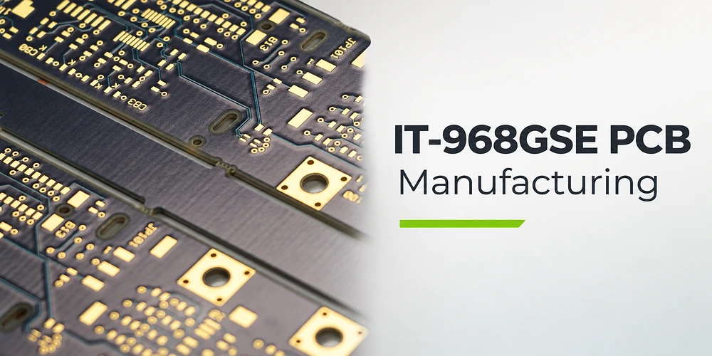
IT-968GSE-piirilevy nopeaan verkkoon
IT-968GSE-piirilevyn kuva erittäin pienihäviöisestä kytkimestä ja...
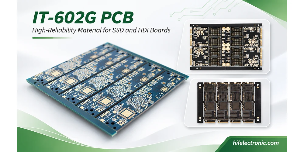
IT-602G HDI -korttien rakentaminen SSD-levyille ja muistimoduuleille
IT-602G piirilevyesimerkkejä HDI-, SSD- ja muistimoduuleille...
Miten saada tarjous piirilevyistä
Suoritetaan DFM/DFA-analyysi puolestasi ja lähetetään sinulle raportti. Voit ladata tiedostosi turvallisesti verkkosivustomme kautta. Tarvitsemme seuraavat tiedot voidaksemme antaa sinulle tarjouksen:
-
- Gerber, ODB++ tai .pcb, sp.
- Tuoteluettelo, jos tarvitset kokoonpanoa
- Määrä
- Käännä aika
Piirilevyjen valmistuksen lisäksi tarjoamme kattavan valikoiman elektroniikkapalveluita, kuten piirilevysuunnittelua, piirilevyasennusta ja kokonaisratkaisuja. Tarvitsetpa apua prototyyppien valmistuksessa, suunnittelun varmentamisessa, komponenttien hankinnassa tai massatuotannossa, tarjoamme kokonaisvaltaista tukea projektisi onnistumisen varmistamiseksi.
Piirilevypalveluita varten toimitathan osaluettelosi (BOM) ja mahdolliset erityiset kokoonpano-ohjeet. Tarjoamme myös DFM/DFA-analyysin suunnitelmiesi valmistettavuuden ja kokoonpanon optimoimiseksi varmistaen sujuvan tuotantoprosessin.