
KB-6167F PCB-laminaat: Productie- en assemblagehandleiding voor betrouwbare meerlaagse printplaten
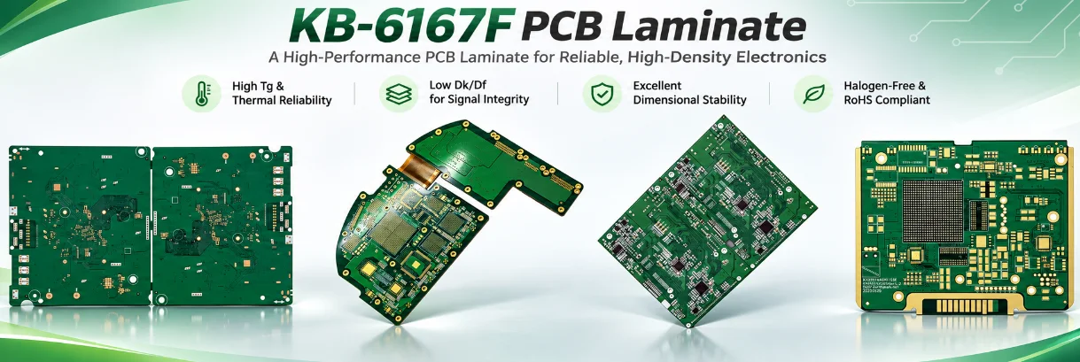

KB-6167F PCB laminate is specified when a multilayer board needs more thermal and dimensional margin than a general-purpose FR-4 construction may provide. Kingboard positions KB-6167F as an FR-4.0 laminate/prepreg system for high-reliability multilayer applications, with high glass-transition temperature (Tg), low Z-axis thermal expansion, lead-free process suitability and anti-CAF capability. For an OEM, however, choosing the laminate is only the starting point: the finished PCB must also meet the approved stackup, drilling, plating, dimensional and inspection requirements.
Highleap Electronics manufactures bare PCBs and assembled PCBAs using customer-approved materials and specifications. We do not manufacture KB-6167F laminate. Our role is to translate the specified material and released design into a controlled PCB fabrication process and, when required, continue through component sourcing, SMT/THT assembly, inspection and project-defined testing.
Why Specify KB-6167F for a Multilayer PCB?
KB-6167F is intended for designs where thermal exposure, layer count or plated-through-hole reliability makes material selection an important part of the PCB construction. Kingboard describes the system as a high-Tg, multifunctional phenolic-cured resin system with inorganic fillers. Its published positioning includes high-layer-count PCBs and lead-free applications.
The practical reason to specify a high-Tg laminate is not simply to obtain a larger Tg number. During multilayer fabrication and lead-free assembly, the PCB experiences multiple heating and cooling cycles. The dielectric, copper layers and plated-hole barrels must remain mechanically compatible through those cycles. A material with controlled Z-axis expansion and suitable thermal resistance can support that design objective, particularly when the board has many layers or a high plated-through-hole count.
What the material choice can—and cannot—do
- Thermal margin: A higher Tg and the published thermal-stress data help engineers assess whether the laminate is appropriate for the planned fabrication and assembly temperature profile.
- Through-hole reliability considerations: Lower Z-axis expansion can reduce one source of thermal strain around plated-through-hole structures, but it does not replace control of drilling, desmear and copper plating.
- Dense multilayer design: The stated anti-CAF capability is relevant when evaluating insulation reliability in designs with closely spaced conductors.
- Loodvrije assemblage: Kingboard positions KB-6167F for lead-free processing; the actual assembly profile and board construction still need to be qualified.
A laminate property is not a finished-board performance guarantee. The result also depends on the core and prepreg combination, glass style, resin content, copper distribution, board thickness, via design and factory process. The material grade should therefore be specified together with the complete PCB construction rather than treated as a standalone purchasing description.
For projects that already have a defined material grade, Highleap’s PCB-laminaatmateriaalservice supports the review of customer-specified laminate systems and their use in the finished board construction.
KB-6167F Material Properties and Published Technical Data
The published KB-6167F data provides useful reference points for material selection. The figures below should be read with their stated test conditions and should not be substituted for the latest manufacturer specification or a production stackup calculation.
| Eigendom | Gepubliceerde referentie | Why it matters to the PCB |
|---|---|---|
| DSC Tg | 175°C typical; specification value at least 170°C under the stated condition | Helps assess the laminate’s thermal transition behavior during fabrication and assembly. |
| Z-as CTE | Alpha 1: 40 ppm/°C typical; Alpha 2: 230 ppm/°C typical | Relevant to dielectric expansion and the thermal strain experienced by plated-through-hole structures. |
| Z-as-uitbreiding | 2.6% typical from 50–260°C | Provides another reference for evaluating dimensional change over a specified temperature range. |
| Thermische weerstand | T-260: greater than 60 minutes; T-288: greater than 35 minutes, typical | Supports comparison of thermal-stress performance under the stated TMA method. |
| Diëlektrische constante (Dk) | 4.8 at 1 MHz; 4.6 at 1 GHz | A material-level reference for signal design; actual impedance depends on the finished stackup and geometry. |
| Verliesfactor (Df) | 0.015 at 1 MHz; 0.016 at 1 GHz | Useful for material comparison, but not a substitute for design-specific signal-integrity analysis. |
| Other stated characteristics | Anti-CAF capability, lead-free suitability and dimensional stability | Relevant to the design’s insulation, thermal and manufacturing objectives; confirm against the approved material data. |
The Dk and Df values above are reported for the stated etched, 50% resin-content test condition. They are not universal values for every core, prepreg or pressed dielectric thickness. For controlled-impedance designs, the fabricator should work from the approved construction and target impedance rather than applying a generic FR-4 value.
How to Translate KB-6167F into a PCB Stackup
A KB-6167F PCB should be defined by its complete stackup, not by the laminate name alone. The finished dielectric geometry is determined by the combination of cores, prepregs, glass styles, resin content, copper weights and lamination conditions. These details affect final board thickness, impedance, registration and manufacturing yield.
Stackup details to release before fabrication
- Layer count, layer sequence and copper distribution
- Approved KB-6167F core construction and core thickness
- Prepreg type, glass style and required pressed dielectric thickness
- Gewichten van koper in de binnen- en buitenlaag
- Afgewerkte plaatdikte en tolerantie
- Reference planes and critical signal-layer assignments
- Controlled-impedance targets and tolerances, where applicable
- Via structure, drill sizes, aspect-ratio constraints and finished-hole requirements
- Surface finish and any customer-specific fabrication or inspection requirements
Controlled impedance requires the actual pressed construction
For a controlled-impedance board, dielectric thickness, copper thickness, trace width, spacing and the selected reference plane all affect the finished impedance. The published material Dk is an input to engineering review, not a complete impedance specification. Highleap’s materiaalselectie voor snelle printplaten approach can help connect the material requirement with the electrical targets of the design.
Highleap's PCB-laagopbouwtechniek capability can also support review of the physical construction before production. This is useful when an OEM has an existing KB-6167F design that needs to be translated into a manufacturable core/prepreg schedule.
If the design specifies a different Kingboard grade, such as KB-6168LE, it should be treated as a separate material and construction approval. KB-6168LE dunne-laag printplaatproductie should not be treated as an automatic substitute for KB-6167F based only on the family name.
Manufacturing Controls for a KB-6167F PCB
A high-performance laminate does not remove the need for process control. The approved stackup must be reproduced through lamination, drilling, hole preparation, plating and final inspection. For a material-specific multilayer PCB, these operations should be reviewed as one connected manufacturing chain.
| Productiefase | Belangrijke controlepunten | Waarom dit zo belangrijk is |
|---|---|---|
| DFM- en stackup-review | Annular rings, drill-to-copper spacing, copper balance, thickness and registration feasibility | Identifies design or construction risks before tooling and volume production. |
| Lamineren | Approved core/prepreg schedule, press construction, dielectric build and layer registration | Keeps the manufactured multilayer structure aligned with the released stackup. |
| Doorboringen en geplateerde gaten | Drill quality, hole-wall preparation, desmear and copper plating | Supports interconnection quality through the multilayer dielectric. |
| Fabrication verification | AOI, electrical testing, dimensional checks and impedance verification when specified | Provides evidence that the finished board meets the released drawing and acceptance criteria. |
Lamination and layer registration
The approved core and prepreg schedule must be translated into a practical press construction. Dielectric build, copper balance and registration need to be considered together, particularly on high-layer-count boards. Highleap’s PCB-lamineringsproces: is part of the manufacturing route used to control multilayer bonding and layer alignment.
Drilling, desmear and copper plating
Low Z-axis expansion is relevant to plated-through-hole design, but the finished interconnection also depends on drill quality, hole-wall preparation, desmear and copper plating. The material’s thermal characteristics should therefore be considered alongside the via design and the fabricator’s process controls.
DFM and final inspection
A PCB DFM-review should take place before tooling release. For a KB-6167F multilayer board, the review should check the proposed stackup, annular rings, drill-to-copper spacing, copper balance, board thickness and registration requirements. Depending on the customer’s specification, final verification may include AOI, electrical testing, dimensional inspection and impedance testing where required. Highleap’s PCB-fabricageservice covers the manufacturing route from production data through agreed inspection and testing.
The objective is repeatability: the specified material, approved construction, production process and inspection plan must describe the same board.
Lead-Free Processing, Thermal Reliability and Applications
Kingboard positions KB-6167F for lead-free PCB designs and high thermal reliability. Its published Tg, Z-axis expansion and T-260/T-288 reference values can help engineers assess whether the material is a candidate for a board exposed to elevated processing temperatures. They do not, by themselves, qualify the complete PCB or PCBA for a particular service environment.
Evaluate the complete thermal profile
A PCB experiences multiple thermal stages during fabrication and assembly rather than one isolated temperature. The dielectric, copper and plated-hole structures respond differently as the board heats and cools. Tg, Z-axis CTE, total Z-axis expansion and thermal-stress data should therefore be considered together with the actual lamination and soldering profiles.
The published material information also identifies dimensional stability, low moisture absorption and anti-CAF capability. These characteristics may support the reliability objectives of dense multilayer designs, but the finished product still needs to be evaluated against its operating environment, electrical design and qualification requirements.
Applications identified in the published material information
The referenced Kingboard information lists consumer electronics, automotive electronics, instruments and power supplies among the application areas. Other Kingboard material information referenced for high-layer-count constructions also identifies high-end servers and wireless communication infrastructure. These are application references, not a guarantee that every design in those categories is suitable without engineering review.
For industrial control, instrumentation and power-related products, Highleap’s industriële PCB-productie capability can be aligned with the customer’s approved KB-6167F construction and fabrication requirements.
KB-6167F PCB Fabrication and PCBA with Highleap
Once the laminate, stackup and fabrication requirements are approved, the project needs a supplier that can manufacture the board to the released specification. Highleap Electronics provides PCB fabrication and PCB assembly, allowing customers to manage the bare-board and assembly stages through one manufacturing partner when that scope is required.
Voor de fabricage van kale printplaten
The manufacturing package should identify KB-6167F and include the approved core/prepreg construction, layer stackup, copper weights, finished board thickness, surface finish, drill data, impedance requirements and inspection criteria. Any proposed alternative material or construction should be submitted for customer review and approval before production; a similar material name or nominal property is not sufficient authorization for substitution.
Voor PCB-assemblage en afgewerkte PCBA's
Highleap's PCB-montageservice can extend the project from the fabricated board to SMT and THT assembly, inspection and testing according to the customer’s requirements. The PCB revision, BOM, placement data and assembly drawings should remain synchronized with the approved bare-board revision.
For customers who want one supplier to coordinate fabrication, component sourcing and assembly, kant-en-klare PCB-assemblage provides an integrated route from PCB manufacturing through component procurement, assembly and testing. The required material grade remains a customer-approved specification within that manufacturing package.
RFQ Checklist and Frequently Asked Questions
What should an OEM include in a KB-6167F PCB RFQ?
| Offerteaanvraagitem | Te verstrekken informatie: |
|---|---|
| PCB design data | Gerber or ODB++, fabrication drawing, drill files and revision. |
| Materiaal en stapeling | KB-6167F requirement, approved core/prepreg construction, layer count, copper weights and finished thickness. |
| Elektrische vereisten | Controlled-impedance targets, tolerances, critical nets and via requirements, where applicable. |
| Kwaliteitseisen | Surface finish, inspection criteria, electrical test requirements and any customer-specific acceptance standard. |
| Omvang van de assemblage | BOM, centroid/placement file, assembly drawing, programming and functional-test requirements if PCBA is needed. |
| Commerciële details | Prototype and production quantities, forecast, delivery target and destination. |
Does Highleap manufacture KB-6167F laminate?
No. Highleap manufactures bare PCBs and PCBAs using customer-approved materials and specifications. KB-6167F is the specified laminate system; it is not a laminate product manufactured by Highleap.
Can KB-6167F be used for lead-free PCB assembly?
Kingboard positions KB-6167F for lead-free processing. The OEM and manufacturer should still review the approved stackup, fabrication process and actual assembly thermal profile before production release.
Are the published Dk and Df values sufficient for controlled-impedance design?
No. They are material-level reference values under stated test conditions. Controlled impedance depends on the complete pressed dielectric construction, copper thickness, trace geometry and reference-plane arrangement. The released stackup and design-specific calculation should govern production.
Can KB-6167F be replaced by another Kingboard material?
Not without customer approval. A different grade, including KB-6168LE, must be reviewed as a separate material and construction. The supplier should not make a substitution based only on a similar product-family name or a small number of published properties.
Highleap Electronics • PCB-productie & PCBA
Vraag een beoordeling aan van de productie van de KB-6167F printplaat.
Send your Gerber or ODB++ files, approved stackup, KB-6167F material requirement, drill data and quantity. If assembly is required, include the BOM and placement data. Highleap can review the manufacturing scope and quote the required bare PCB or PCBA production.

aanbevolen berichten
TMM PCB-fabricage
Inhoudsopgave TMM PCB-fabricagebereik voor RF en...

RT duroid 6002 PCB-offerte en stapeling
Deze pagina is verantwoordelijk voor de taak 'citaat en stapeldefinitie'...
TMM6 filter printplaatproductie
Inhoudsopgave: Waarom ontwerpers van magnetronfilters gebruikmaken van...
Taconic RF 35 versus RO4350B printplaat
Inhoudsopgave RF-35 versus RO4350B Inkoop en...
Hoe vraag ik een offerte aan voor printplaten?
Wij voeren graag een DFM/DFA-analyse voor u uit en sturen u vervolgens een rapport. U kunt uw bestanden veilig uploaden via onze website. Om u een offerte te kunnen geven, hebben we de volgende informatie nodig:
-
- Gerber, ODB++ of .pcb, spec.
- BOM-lijst als u assemblage nodig heeft
- Aantal
- Draaitijd
Voor PCBA-diensten verzoeken wij u uw BOM (Bill of Materials) en eventuele specifieke assemblage-instructies te verstrekken. Wij bieden ook DFM/DFA-analyses aan om uw ontwerpen te optimaliseren voor maakbaarheid en assemblage, wat een soepel productieproces garandeert.