
MEGTRON M PCB-productie voor snelle meerlaagse toepassingen
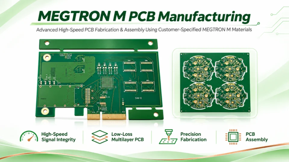

Choosing a laminate for high-speed data transmission is only the starting point. To manufacture a reliable MEGTRON M PCB, the PCB manufacturer must translate the material specification into a controlled multilayer construction, including the stackup, dielectric thicknesses, copper configuration, impedance targets, drilling, lamination and inspection requirements.
Highleap Electronics manufactures multilayer PCBs and provides PCB assembly using customer-specified high-performance materials, including Panasonic MEGTRON M. For projects specifying R-5735 laminate and R-5630 prepreg, our role is to review and manufacture the board to the approved material and fabrication requirements. Highleap is a PCB/PCBA manufacturer, not a manufacturer of Panasonic laminate.
Panasonic identifies MEGTRON M as a low-transmission-loss, highly heat-resistant multilayer circuit board material for high-speed and large-volume data transmission. Its stated application areas include servers, routers, ICT infrastructure equipment, supercomputers, measuring instruments and antennas. For server projects, server motherboard PCB manufacturing must also account for routing density, connector loads and assembly constraints.
What matters when sourcing a MEGTRON M PCB?
- Confirm the specified material combination: R-5735 laminate and R-5630 prepreg.
- Release the complete stackup, copper weights and finished dielectric requirements.
- Define impedance targets, via structures and backdrilling requirements where applicable.
- Align fabrication inspection and any PCBA testing with the finished-board requirements.
MEGTRON M PCB Material System: R-5735 Laminate and R-5630 Prepreg
MEGTRON M is a Panasonic multilayer circuit board material system. This article focuses on projects specifying the following combination:
- R-5735: laminaat
- R-5630: prepreg
The distinction between laminate and prepreg matters when a PCB stackup is prepared for production. The material name alone does not define the finished board. The manufacturer also needs the approved core and prepreg construction, dielectric thicknesses, copper weights, layer assignments and lamination requirements.
A MEGTRON M PCB should therefore be reviewed as a complete meerlaagse constructie, not simply as a material purchasing requirement. If the material has not yet been finalized, Highleap’s Technische ondersteuning bij materiaalselectie voor printplaten can help relate the material requirement to the intended PCB design.
R-5735 Material Properties and Published Technical Data
The following figures are representative values for Panasonic R-5735 as provided in the source material for this article. They are useful for initial material review, but they should always be checked against the latest applicable Panasonic documentation and its stated test methods.
| Eigendom | R-5735 typical value |
|---|---|
| Tg, DSC | 195 ° C |
| Td, TGA | 360 ° C |
| T288 met koper | 35 min |
| CTE α1, Z-as | 31 ppm / ° C |
| CTE α2, Z-as | 240 ppm / ° C |
| Dk bij 13 GHz | 3.75 |
| Df bij 13 GHz | 0.0087 |
| Waterabsorptie | 0.14% |
| Schilsterkte, 1 ounce koper | 1.3 kN / m |
| Ontvlambaarheid | 94V-0 |
Belangrijk: These are typical material values, not guaranteed performance values for every finished PCB. Actual results depend on the selected core and prepreg construction, glass style, resin content, pressed dielectric thickness, copper configuration, fabrication process and measurement conditions.
How should engineers interpret the data?
- Thermische eigenschappen: Tg, Td and T288 provide reference points for reviewing thermal behavior. They do not independently qualify a finished PCB for a specific assembly profile or service environment.
- Z-axis expansion: CTE data is relevant when evaluating multilayer structures and plated through-hole reliability. Drilling, desmear, plating and the finished via structure remain important manufacturing controls.
- Elektrische eigenschappen: Dk and Df at 13 GHz are material-level reference values under specified test conditions. They should not be used as universal values for every pressed dielectric construction.
- Moisture and insulation considerations: Water absorption and the material’s stated characteristics can inform design review, but finished-board qualification must reflect the actual product requirements.
MEGTRON M PCB Stackup Design
For a high-speed multilayer PCB, the stackup affects electrical behavior and manufacturing feasibility—not just the layer count. Signal layers, reference planes, dielectric thickness, copper thickness, trace geometry, prepreg construction and layer symmetry all need to be considered together.
Stackup information to define before fabrication
- Aantal lagen en volledige lagenvolgorde
- Approved R-5735 laminate and R-5630 prepreg construction
- Core thickness, prepreg type and required pressed dielectric thickness
- Gewichten van koper in de binnen- en buitenlaag
- Afgewerkte plaatdikte en tolerantie
- Signal-layer assignments and reference-plane locations
- Doelwaarden en toleranties voor gecontroleerde impedantie, indien van toepassing
- Via types, drill sizes, aspect ratios and finished-hole requirements
- Backdrill requirements and depth tolerances, if specified
- Surface finish and customer-specific inspection criteria
For controlled-impedance designs, the final pressed dielectric thickness and actual copper geometry matter more than a standalone material Dk figure. Highleap’s PCB-laagopbouwtechniek process helps translate electrical requirements into a manufacturable multilayer construction.
This review is especially important when a customer transfers an existing design from another PCB manufacturer. Available prepreg combinations, copper thicknesses and process tolerances may differ. The objective is not to change the design unnecessarily, but to confirm that the released construction can be reproduced consistently.
Controlled Impedance and Signal Integrity for MEGTRON M PCBs
MEGTRON M is positioned for high-speed data transmission, so controlled impedance may be a key part of the PCB fabrication specification. However, specifying a laminate with a published Dk value does not, by itself, establish the impedance of a finished trace.
A controlled-impedance design may require the manufacturer to review:
- Target single-ended and differential impedance
- Trace width, spacing and finished copper thickness
- Dielectric height and reference-plane location
- Copper roughness and the selected copper foil
- Differential-pair geometry and routing layer
- Manufacturing tolerances and impedance test method
- Test coupon design and acceptance limits, where required
For example, a 50-ohm single-ended target or a differential impedance target cannot be guaranteed simply because the laminate has a specified Dk. The finished PCB geometry and dielectric construction determine the transmission-line characteristics.
Highleap's PCB-productie met gecontroleerde impedantie service supports impedance review and testing requirements for high-speed and RF designs. For an MEGTRON M project, include the target impedance, relevant layers, tolerances and test requirements in the fabrication documentation so they can be reviewed before production.
What Should a MEGTRON M PCB Manufacturer Review Before Production?
Material availability is only one part of a material-specific PCB project. Before production, the manufacturer should review the complete data package and check that the electrical, mechanical and fabrication requirements are compatible.
1. Material specification
Identify the required material system clearly as Panasonic MEGTRON M R-5735/R-5630. Avoid relying on a generic description such as “high-speed material.” Any proposed material or construction alternative should be submitted for customer approval before production.
2. Layer stackup and board thickness
Check the layer sequence, core and prepreg construction, copper weights, dielectric thicknesses and finished board thickness against the released design requirements.
3. Impedance requirements
Confirm target impedance values, signal layers, trace geometry, tolerances, test coupons and the required verification method. Impedance should be planned during stackup and CAM review, not treated as an after-production correction.
4. Drill and via structure
Review drill sizes, aspect ratios, plated and non-plated holes, via structures and any controlled-depth drilling requirements. These details can affect manufacturability and the reliability of multilayer interconnections.
5. Copper distribution and lamination
Uneven copper distribution can influence lamination behavior, dielectric thickness and board flatness. Signal routing should be considered together with power and ground-plane structures when reviewing the complete construction.
6. DFM, tolerances and inspection
Check whether dimensional tolerances and design clearances are compatible with the intended process. Highleap’s PCB-ontwerp voor productie (DFM) beoordeling can help identify issues before tooling and fabrication begin.
MEGTRON M PCB Manufacturing Process
A material-specific multilayer PCB should follow a controlled manufacturing workflow. Depending on the approved construction, a typical process may include:
Engineering Review → CAM Preparation → Material Preparation → Inner-Layer Imaging and Etching → Lay-up and Lamination → Drilling → Desmear and Plating → Outer-Layer Imaging and Etching → Surface Finish → Inspection → Electrical Testing → Final Inspection
The exact sequence and process controls depend on the board design. A conventional multilayer MEGTRON M PCB may require a different process plan from a high-layer-count board with complex via structures or backdrilling.
Highleap biedt PCB-fabricage op maat for multilayer and high-performance PCB designs. The manufacturing plan should be matched to the customer’s approved material construction, stackup, tolerances and inspection requirements rather than forcing every project into a standard process flow.
MEGTRON M PCB Backdrilling and Via-Stub Control
In some high-speed multilayer designs, a through-hole via leaves an unused section of plated barrel beyond the layer where the signal transitions. This unused section is commonly called a via stub and can affect signal integrity at high frequencies.
When the electrical design requires it, terugboren can remove the unnecessary portion of the plated via and reduce the electrical impact of the stub. It should not be added automatically to every MEGTRON M PCB. Its suitability depends on the signaling requirements, layer transitions, via structure, channel design and electrical analysis.
When backdrilling is specified, the fabrication package should define the target depth, allowable residual stub and relevant drill tolerances. Highleap supports PCB-achterboring en gecontroleerde diepteboring voor meerlaagse hogesnelheidsprintplaten.
MEGTRON M PCB Applications: Servers, Routers and Communication Electronics
Panasonic lists MEGTRON M for applications including network equipment, wireless communication, ICT infrastructure equipment, supercomputers, measuring instruments and antennas. These products may require multilayer construction, high-speed signal transmission, controlled impedance, dense routing, stable reference planes and reliable plated through-holes.
For server and networking projects, the material selection should be considered together with board architecture, connector interfaces, component density, thermal conditions and assembly requirements. Highleap’s hoogfrequente en snelle PCB-productie capabilities cover specialized multilayer and RF PCB constructions.
The application name alone does not determine whether a material is suitable. The complete electrical design, mechanical construction, operating environment and qualification requirements should guide the final material and manufacturing review.
MEGTRON M PCB-assemblage: van kale printplaat tot complete PCBA
For many OEM projects, bare-board fabrication is only one stage of the supply chain. If the MEGTRON M board also requires component placement, Highleap can provide PCB assembly as part of the manufacturing workflow.
Highleap's PCB-assemblagediensten: include SMT and through-hole assembly, component sourcing, AOI, X-ray inspection, electrical testing and functional testing options, according to project requirements.
For high-speed communication boards, the transition from bare PCB to PCBA may require attention to:
- BGA placement and fine-pitch component assembly
- Solder-joint quality and inspection coverage
- Component traceability and sourcing requirements
- Assembly thermal profile and board warpage
- X-ray inspection and functional testing, where specified
Keeping PCB fabrication and assembly within one manufacturing workflow can simplify communication between the bare-board and assembly stages. The PCB revision, BOM, placement data and assembly drawings should remain aligned with the approved board revision.
MEGTRON M PCB Manufacturing with Highleap
Highleap Electronics is a PCB manufacturer and PCBA provider—not a Panasonic laminate manufacturer. For MEGTRON M projects, our role is to manufacture customer-specified boards using the approved R-5735 laminate and R-5630 prepreg construction, subject to material availability and engineering review.
Depending on the project scope, our manufacturing services include:
- Multilayer and high-speed PCB fabrication
- Productie van hoogfrequente en RF-printplaten
- Stackup and controlled-impedance review
- HDI en complexe interconnectiestructuren
- Backdrilling and controlled-depth drilling
- DFM-technische beoordeling
- SMT- en doorsteekmontage van printplaten
- Component sourcing, AOI and X-ray inspection
- Electrical and functional testing options
Customers requiring fabrication and assembly can also use Highleap’s kant-en-klare PCB-assemblage service to coordinate PCB manufacturing, component procurement, assembly and testing through one workflow. Prototype, pilot and production requirements should be reviewed against the actual design package and order scope.
What to Include in a MEGTRON M PCB Manufacturing RFQ
To assess a MEGTRON M PCB project accurately, provide the relevant design files and manufacturing requirements at the quotation stage.
| Omvang van de offerteaanvraag | Te verstrekken informatie: |
|---|---|
| PCB-fabricage | Gerber or ODB++ files, drill files, fabrication drawing, stackup, board thickness, copper weights, R-5735/R-5630 material specification, surface finish and quantity. |
| Elektrische vereisten | Impedance targets and tolerances, controlled layers, test coupon requirements, via structure and backdrill specifications, if applicable. |
| PCB-montage | BOM, pick-and-place/CPL file, assembly drawings, component part numbers, assembly quantity and inspection requirements. |
| Testen en levering | Electrical or functional test requirements, programming details if applicable, delivery target and destination. |
Als het ontwerp al specificeert MEGTRON M R-5735/R-5630, state the material requirement clearly in the fabrication notes. If the stackup is not finalized, provide the layer count, target board thickness, copper weights and electrical requirements so the construction can be reviewed before production.
Highleap Electronics · PCB-productie & PCBA
Request a MEGTRON M PCB Manufacturing Review
Send your Gerber or ODB++ files, approved R-5735/R-5630 material requirement, stackup, drill data and quantity. If assembly is required, include the BOM and placement files. Highleap can review the manufacturing scope and prepare a quotation for the required PCB or PCBA.
Vraag een offerte aan voor een MEGTRON M printplaat
Discuss PCB Assembly
Veelgestelde vragen over MEGTRON M printplaten
Is MEGTRON M a PCB laminate material?
MEGTRON M is a Panasonic multilayer circuit board material system. This article covers projects specifying R-5735 laminate with R-5630 prepreg. Highleap manufactures PCBs using customer-specified materials; it does not manufacture the Panasonic laminate.
What are R-5735 and R-5630?
R-5735 is the laminate identified for the MEGTRON M construction discussed here, while R-5630 is the associated prepreg. The approved core/prepreg combination and pressed dielectric construction should be stated in the production stackup.
What is the Dk of Panasonic R-5735?
The typical Dk value listed in the source material is 3.75 op 13 GHz under the stated test conditions. It is a material reference value, not a universal Dk for every finished PCB construction.
What is the Df of MEGTRON M R-5735?
The typical Df value listed in the source material is 0.0087 op 13 GHz under the stated test conditions. Confirm the applicable Panasonic documentation and test method when using the value for design calculations.
What is the Tg of R-5735?
The published typical DSC Tg value listed in the source material is 195 ° C. Other thermal data, including T288 with copper, should also be reviewed under the relevant test conditions.
Kan Highleap MEGTRON M meerlaagse printplaten produceren?
Highleap manufactures multilayer PCBs using customer-specified high-performance materials, including MEGTRON-series materials. The exact material construction, availability, stackup and manufacturing requirements must be reviewed against the customer’s fabrication data before production.
Kan Highleap MEGTRON M-printplaten assembleren?
Yes. Highleap provides PCB assembly options including SMT, through-hole assembly, component sourcing, AOI, X-ray inspection, electrical testing and functional testing, according to the project requirements.
Does every MEGTRON M PCB require backdrilling?
No. Backdrilling is design-dependent. It should be specified when signal-integrity analysis and the via structure show that reducing the via stub is necessary.
How can I request a MEGTRON M PCB quotation?
Submit your Gerber or ODB++ files, drill files, stackup, material specification, board quantity, impedance requirements and special fabrication notes. If assembly is required, also provide the BOM, placement file and assembly drawings. You can start through Highleap’s PCB-offertepagina.

aanbevolen berichten
TMM PCB-fabricage
Inhoudsopgave TMM PCB-fabricagebereik voor RF en...

RT duroid 6002 PCB-offerte en stapeling
Deze pagina is verantwoordelijk voor de taak 'citaat en stapeldefinitie'...
TMM6 filter printplaatproductie
Inhoudsopgave: Waarom ontwerpers van magnetronfilters gebruikmaken van...
Taconic RF 35 versus RO4350B printplaat
Inhoudsopgave RF-35 versus RO4350B Inkoop en...
Hoe vraag ik een offerte aan voor printplaten?
Wij voeren graag een DFM/DFA-analyse voor u uit en sturen u vervolgens een rapport. U kunt uw bestanden veilig uploaden via onze website. Om u een offerte te kunnen geven, hebben we de volgende informatie nodig:
-
- Gerber, ODB++ of .pcb, spec.
- BOM-lijst als u assemblage nodig heeft
- Aantal
- Draaitijd
Voor PCBA-diensten verzoeken wij u uw BOM (Bill of Materials) en eventuele specifieke assemblage-instructies te verstrekken. Wij bieden ook DFM/DFA-analyses aan om uw ontwerpen te optimaliseren voor maakbaarheid en assemblage, wat een soepel productieproces garandeert.