
PCB FABRICATION + PCBA
14-kerroksinen piirilevykokoonpano ja yhden luukun piirilevyjen valmistus
Highleap Electronics tarjoaa 14 layer PCB fabrication and assembly coordination in China, covering custom bare-board manufacture and the agreed stages needed to deliver populated PCBAs. High-density FPGA modules, network interface cards and industrial control electronics often combine fine-pitch BGAs, high-speed traces, multiple voltage rails and mixed SMT/THT hardware.
Send your Gerber or ODB++ files, stackup, target quantity and inspection requirements. Add the BOM for assembly.
14 Layer PCB Assembly: From Fabrication to Tested PCBA
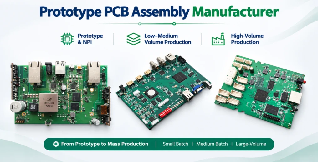
Highleapin PCB assembly and turnkey EMS offering includes SMT, through-hole assembly, component sourcing, IC programming, coating options and customer-defined test work. For a fourteen-layer assembly, these services need to follow a single controlled hardware revision. The bare-board layer count and fabrication features are assessed under Highleap’s 14-layer PCB manufacturing scope before assembly tooling is confirmed. A release-ready quotation distinguishes which party owns the bare PCB, BOM procurement, specialist assembly operations, programming fixtures and functional-test limits.
| suorite | Minimum release definition | What Highleap can coordinate |
|---|---|---|
| Bare 14-layer PCB | Approved physical stackup, hole/cap structure, copper, finish, e-test class | Fabrication and board-level quality acceptance |
| Komponenttimateriaali | Manufacturer part numbers, AVL, fitted/DNP variants, permitted substitutes | Approved purchasing, kit receiving and shortage reporting |
| SMT/THT process | Centroid/XY data, drawings, polarity, paste/process constraints | Stencil, placement and appropriate joining processes |
| Software and configuration | Firmware file/version, programming interface, security/serialization rules | Programming and identification under an agreed method |
| PCBA acceptance | AOI/X-ray/ICT/FCT scope, test limits, evidence and packaging | Inspection and project-defined functional-test execution |
A single commercial contact does not mean the same production line performs fabrication, coating, programming and every product-level qualification. The actual service and any specialist partner should be specified. If the order calls for fully assembled units, enclosure, harness, potting or labeling, those are separately identifiable box-build deliverables, not implicit in the bare PCBA price.
Can Highleap deliver a complete 14-layer PCBA rather than a bare board?
Yes, subject to a compatible design package and agreed material, assembly and test responsibilities. A fabricated and electrically tested fourteen-layer PCB is not yet a functional electronic product. The PCBA release needs the fitted BOM, placement data, manufacturing notes, programming and acceptance. The quotation should state the hardware revision and whether each unit receives functional test or the inspection plan uses defined sampling.
What is included in a full-turnkey 14-layer PCBA order?
One coordinated project can include multilayer PCB fabrication, procurement of approved BOM components, SMT population, through-hole operations, firmware programming and board-level inspection or functional test. Each activity has a separate manufacturing responsibility and acceptance requirement. Highleap’s turnkey PCB assembly scope supports a single project interface without implying that every specialist operation is performed on the same line.
The bare-board fabrication release covers the approved fourteen-layer stackup, finished copper, drilled interconnects, pad finish, mask, outline and electrical-test acceptance. The assembly release covers actual fitted parts, polarity, stencil, placement, soldering process, programming and the product-specific checks defined by engineering. Keeping these releases coordinated is particularly valuable where BGA lands contain capped microvias or connectors require controlled hole dimensions.
What is included in a turnkey 14-layer PCBA quotation?
The quote can cover the approved bare PCB, BOM sourcing, assembly labor and setup, any stencils/fixtures, agreed inspection, programming, functional test and packaging. It should identify excluded tooling, customer-supplied components or special operations. Highleap can also quote partial turnkey and consigned models, with a clear division of procurement responsibility.
Industrial and Network 14-Layer PCB Assemblies
Highleap can evaluate populated fourteen-layer boards for industrial Ethernet switches, gateway controllers, FPGA/SoC carrier boards, embedded computing modules, data acquisition cards, machine-vision electronics, instrumentation controllers and high-speed network interfaces. The intended assembly must be identified by product requirements, not by calling the board “complex.”
- Network and communication boards can require a defined SerDes connector, tight component land geometry, low-noise clocks, power sequencing, boot images and traffic/interface checks. A board with perfectly soldered parts can still fail the end-system link test if the connector, fixture or firmware is not controlled.
- FPGA and processor boards may include large BGAs, DDR memory, flash, high-speed connectors and multiple regulators. Verify BOM variants, BGA hidden-joint evidence, programming and supply-rail checks; full signal-training acceptance is project-specific.
- Teollisuuden ohjaus PCBA can combine processors with isolated I/O, optocouplers, relays, through-hole terminals and heavy mechanical connectors. Test requirements may include channel continuity, isolation, firmware configuration and defined environmental or load limits.
- Mixed-signal measurement boards may place sensitive analog paths near digital and power devices. Cleaning, residue limits, ESD handling, shielding and calibrated measurement need to be defined where the application makes them important.
A fourteen-layer power or control board should not automatically be represented as an automotive- or medical-certified assembly. The customer must specify regulatory, safety and environmental qualification separately, with applicable evidence from the actual manufacturing and test sites.
Can several related boards be assembled and shipped as one equipment set?
Yes, as an agreed multi-board supply program. A main fourteen-layer processor card, a power daughterboard and a connector/I/O card can have different PCB stackups and acceptance procedures but share a coordinated release, component-sourcing plan and shipment identity. Each board still needs its own revision, BOM and test result; a passed mainboard does not automatically qualify the full equipment set.
BGA, QFN, SMT and Through-Hole Component Assembly

A 14-layer processor or FPGA card may contain fine-pitch BGAs and QFNs alongside shielded connectors, crystals, power inductors and through-hole hardware. Stencil design, solder-paste selection, moisture-sensitive component handling, thermal profiling and inspection are defined by the actual packages. The copper count alone does not determine pick-and-place accuracy or the required reflow profile.
Highleap voi arvostella BGA PCB assembly and inspection requirements for bottom-terminated packages. Visible joints may be inspected with AOI; hidden joints often require X-ray criteria where specified. Neither approach alone confirms high-speed interface function or a programmed FPGA operating correctly. Large thermal masses, double-sided assembly and high-profile connectors must also be considered during panel support and soldering-route planning.
Can SMT and through-hole parts be assembled on the same board?
Yes, with a suitable sequence and joining process. Reflowed SMT components can be followed by selectively soldered, wave-soldered or manually soldered through-hole components as appropriate. The board layout, bottom-side parts, connector design and heat-sensitive devices determine whether each operation is suitable. Press-fit components require their own hole and insertion criteria, not a generic soldering specification.
Why must BGA pad finish, VIPPO and stencil decisions be made before fabrication?
An exposed via inside a solderable BGA land can draw solder into the hole and affect joint volume. A designed via-in-pad plated over (VIPPO) construction needs the approved filling, planarization and copper cap. The manufacturing drawing must identify which pads require this and the tolerance allowed for flatness. The stencil and reflow process then use the finished board condition. A last-minute change from an ordinary through-hole to a capped via is not just a factory tooling adjustment; it can affect the board release, DFM, test and production cost.
A similar interface exists around press-fit connectors: hole wall finish and finished diameter must suit the component manufacturer’s installation requirement. Do not assume a generic PTH tolerance guarantees press-fit acceptance. Board-to-assembly ownership should be settled during the quotation rather than after parts arrive.
DFM and DFA for High-Density Multilayer Assemblies
Early fabrication and assembly reviews prevent common interface problems. A plated-through-hole that is electrically correct may still have the wrong finished diameter for a press-fit terminal. A via placed directly in a BGA solder land may create solder-wicking risk without the specified fill and copper cap. A technically valid stackup may become difficult to assemble if the board or panel deflects during reflow.
Highleap can combine a 14-layer stackup and drill review PCB assembly DFM rules to identify such conflicts before the first manufacturing lot. Required documentation includes the released BOM and alternates, component orientation and centroid data, paste/placement restrictions, solder-mask requirements, panelization and test-point access.
For dense products, high-speed routing and assembly should not be separated into independent assumptions. Via-stub reduction, solderable pad finish, return-path routing and component land pattern changes may each affect both the fabrication drawing and the assembled system verification.
Turnkey BOM Sourcing and Component Supply Chain Control
A fourteen-layer FPGA or network board may be technically producible but commercially blocked by a single allocated BGA, connector or clock device. Highleap can perform a BOM availability review and coordinate approved sourcing, but the design authority must control substitutions and lifecycle changes. A replacement that has the same land pattern can still differ in boot behavior, memory timing, isolation, power demand or qualification status.
A practical procurement register records approved manufacturer part number; authorized source policy; stock/lead status; acceptable alternates; buy quantity and attrition; customer-consigned items; moisture-sensitive handling; date code or traceability requirements; and cost validity. Where a critical part is customer-supplied, specify incoming inspection and who owns shortages, damage and unused stock.
| Hankintamalli | Material ownership and risk | Release requirement |
|---|---|---|
| Täysin avaimet käteen -periaatteella | Highleap sources agreed PCB and approved BOM | AVL, substitution authority, forecast, pricing validity and test scope |
| Osittain avaimet käteen -periaatteella | Customer allocates restricted components; supplier purchases remainder | Kit arrival, inspection, component ownership, excess treatment |
| Määrätty kokoonpano | Customer provides most/all boards or components | Lot identity, MSL packaging, kit count and process feasibility |
For regular production, BOM revisions need to be synchronized with PCB part/revision and firmware variant. This matters for software-configured FPGA boards where a component change may require a different programming image, resistor option or test profile. Production should not proceed on an unapproved mix of hardware and software releases.
Which BOM problems should be resolved before ordering the first board?
Confirm the availability of high-value processors and memory, obsolescence or allocation of critical parts, connector mechanical requirements, component MSL status and any preferred or prohibited substitutions. If parts impose a long supply lead time, align procurement with the approved fourteen-layer stackup release; a completed PCB cannot compensate for an unavailable primary device.
Who approves the BOM and manages component substitutions?
A full-turnkey build uses approved manufacturer part numbers and agreed procurement sources. Partial turnkey allocates selected parts—such as an FPGA, security module or customer-supplied memory—to the OEM while Highleap sources the remainder. A consigned program places greater emphasis on incoming quantity, storage condition, moisture-sensitive packaging, lot identity and unused-material disposition.
| Kokoonpanomalli | Komponentin omistajuus | Ohjauspiste |
|---|---|---|
| Täysin avaimet käteen -periaatteella | Supplier sources approved BOM lines | Source, substitutions and procurement exceptions |
| Osittain avaimet käteen -periaatteella | OEM consigns restricted components | Incoming lot and shortage responsibility |
| Määrätty kokoonpano | OEM provides defined component kit | Completeness, handling and lot traceability |
Highleap voi koordinoida electronic component procurement and BOM review. Component substitutions must follow customer approval. Pin compatibility is not sufficient when alternative devices can change firmware requirements, analog characteristics, power integrity, connector fit or qualification status. Material shortages should be reported with explicit proposed alternates and their engineering impact, not silently resolved at placement.
How are unavailable components handled during PCBA production?
Unapproved substitutes are not fitted as equivalent parts. Highleap can flag supply risk, evaluate authorized sources, and quote accepted alternatives after the product’s design authority approves them. If a component requires a new land pattern or pin assignment, the PCB revision and assembly data must be updated before further boards are built.
Send the controlled PCB files, fitted BOM, centroid, programming and test scope. We can review a coordinated bare-board and assembly quotation with defined procurement and acceptance responsibilities.
Firmware Programming, Conformal Coating and Box-Build Options
Highleap’s published EMS offering includes IC ohjelmointi, muodollinen pinnoite, selected potting operations and finished product assembly. These can be included where specified and qualified for the particular PCBA. A programmer that can load a microcontroller image does not automatically cover secure provisioning of every FPGA, wireless module or hardware-security device. Provide the target IC, programming file, interface, programming station requirements and post-program verification method.
For serialized electronics, decide whether the unit receives a unique ID, MAC address, configuration file, bootloader or production token. Record whether the relevant result is stored against a board serial number, lot number or shipping carton. Some secure provisioning workflows involve customer-owned secrets or protected servers; these require a separate security and data-handling agreement, not an assumed standard firmware service.
Conformal coating requires a released keep-out drawing: connectors, test pads, BGA interfaces, shields, heatsink or mating areas may need masking, while the coating type, coverage, cure, thickness and inspection standard must match the product environment. Potting and underfill are distinct processes with different thermal and rework consequences. These services should be scoped on the assembly drawing and placed after compatible cleaning and test operations.
Does “fully tested” mean each assembly passed an Ethernet or FPGA performance test?
Only when the approved test plan defines that behavior, fixture, conditions and pass/fail limits. An AOI pass and a programmed device do not establish traffic throughput, DDR training, EMC or environmental durability. Highleap can coordinate test execution under a defined procedure; special performance testing needs appropriate fixtures, equipment and acceptance records, potentially supplied by the customer.
AOI, X-Ray and Functional Testing for 14 Layer PCBA

Quality acceptance combines workmanship evidence and circuit-specific operation. Bare-board e-test confirms PCB continuity and isolation. SPI and AOI address specified paste and visible assembly conditions. X-ray can evaluate selected hidden BGA or QFN joint features. Programming confirms the loaded image or configuration using the agreed method; functional testing verifies the defined supply rails, inputs/outputs and interfaces.
Highleap can discuss a PCBA functional-test program with customer pass/fail limits, the required fixture or host software and a report/traceability plan. Some products require Ethernet traffic testing, bootloader verification, calibration, thermal loading or other specialized checks. The actual tools and test limits should be specified before the production order; a general “100% tested” statement is not an adequate test definition.
Can a 14-layer PCB assembly be functionally tested without a customer fixture?
A limited power, programming or interface check may be possible when the test method is defined. Complex networking and FPGA boards may require dedicated fixtures, software, calibrated instruments or load equipment. Test development and routine execution are different services and should be identified separately in the quotation.
Which inspection records confirm an assembled board has passed?
Rather than asking for an unspecified “100% tested” service, include a matrix stating the purpose, method, sampling and report for each assembly check. A reasonable product-specific plan might separate SPI after printing, visible placement/solder AOI, selected BGA X-ray, in-circuit tests where feasible, firmware verification and powered functional tests. Not every board supports all methods or gives them equal risk-reduction value.
| Tarkastusasema | Tyypillinen insinöörikysymys | Scope decision to record |
|---|---|---|
| Bare-board acceptance | Is the manufactured 14-layer netlist correct? | Supplier e-test and any impedance records |
| SMT-tarkastus | Are components oriented and soldered as released? | SPI/AOI scope and workmanship acceptance |
| BGA/X-ray | Are specified concealed joints acceptable? | Which packages, criteria and sampling method |
| Laiteohjelmiston ohjelmointi | Was the correct software/configuration applied? | Image version, checksum or verification log |
| Toimintatesti | Do required rails and interfaces operate? | Fixture, load, limits, test coverage and traceability |
| Packing/release | Is the shipment the correct hardware variant? | Serial/lot labels, BOM revision, ESD protection and report set |
When transitioning from an engineering sample to production, retain a controlled first-article assembly result. Rework, substitution and component shortage exceptions should have an approval path. The OEM’s product qualification and regulatory testing remain separate from board-level acceptance unless expressly included in the project.
14 Layer PCB Prototype Assembly and Production Release
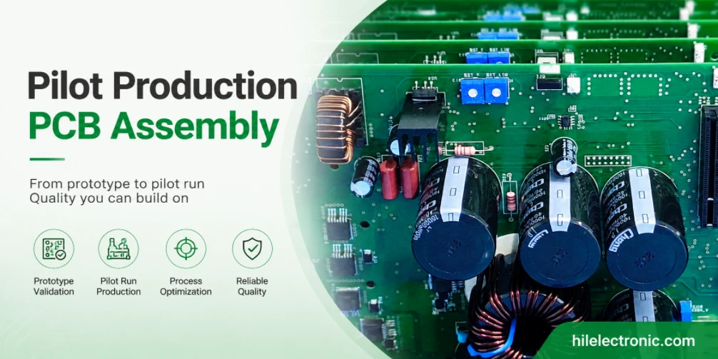
The first populated boards should verify the approved fabrication revision, fitted BOM, stencil and process configuration, connector interfaces, firmware and functional-test evidence. In repeat manufacturing, the accepted hardware and software variants must remain identifiable, especially when several BOM options share the same fourteen-layer PCB.
Highleap voi koordinoida Piirilevykokoonpanon tuotannon siirto with an existing released product, including material responsibility, known process issues and available test fixtures. The production records should define the first-article scope, engineering deviations, rework authorization and lot or serial identification where required.
For a new design, an earlier 14-layer prototype build can confirm bare-board construction and acceptance before the populated pilot. Prototype success does not automatically qualify every material, fixture or process change during later manufacturing.
14 Layer PCBA Cost, Lead Time and Delivery Planning
The delivered PCBA price includes several different cost categories: bare-board fabrication, approved BOM components, SMT/THT processing, packaging and any agreed programming or testing. Fine-pitch BGA inspection, custom fixtures, conformal coating or box-build activities are separately scoped when specified. Material availability can affect the assembly schedule independently of the PCB fabrication lead time.
Highleapin 14-layer PCB manufacturing cost analysis explains bare-board cost drivers. For the populated assembly, provide the approved BOM, quantity forecast, acceptable component alternatives and final test requirements so material procurement and assembly time can be estimated against a real release.
What determines the total delivered PCBA price and schedule?
The manufacturing schedule for an assembled fourteen-layer board includes fabrication release, bare-board production and inspection, component availability, stencil/fixture preparation, SMT/THT execution, programming, functional test and dispatch. These stages are not always strictly sequential: approved BOM procurement may start in parallel with bare-board fabrication, while a custom test fixture may need lead time before boards are populated. The quotation should identify the critical path and which approval or component is holding the schedule.
A complete cost comparison should separate PCB fabrication, BOM sourcing, assembly processing, one-time tooling and test development, routine test execution, coating or box-build, programming and logistics. A low bare-board price may not yield a competitive tested-PCBA cost if the supplier cannot support the required BGA, fixture or firmware workflow. Highleap’s one-stop offer is strongest when these responsibilities can be coordinated on a released manufacturing package with clearly documented boundaries.
What is required to obtain a production quote rather than a rough assembly estimate?
Submit controlled Gerber/ODB++ files and approved physical stackup; drill and via-fill callouts; full BOM and AVL; centroid/placement data; assembly drawing and solder process constraints; firmware and programming instructions; test fixture or functional specification; sample/production quantities; and packing/destination terms. State which special operations are mandatory and which are options. The response can then distinguish firm items from unresolved NRE or qualification work.
Request a Complete 14 Layer PCB Assembly Quote
For a coordinated quotation, send Gerber/ODB++ or IPC-2581, drill and special-feature files, the approved 14-layer stackup and finish specification, BOM with manufacturer part numbers, centroid/XY positions, assembly drawings, fitted/DNP variants, firmware or programming instructions and available functional-test procedures. Indicate prototype and production quantities, delivery location, component ownership and special packaging requirements.
Highleap can then define the bare-board route and the populated-board work in one proposal, with the agreed inspection and test boundaries recorded before release.
Include the PCB construction, approved parts, SMT/THT drawings, firmware and electrical test requirements, plus the required prototype and production quantities.

suositeltava Viestejä
Prototyyppien piirilevykokoonpanon valmistaja
Highleap Electronics on prototyyppinen piirilevykokoonpano...
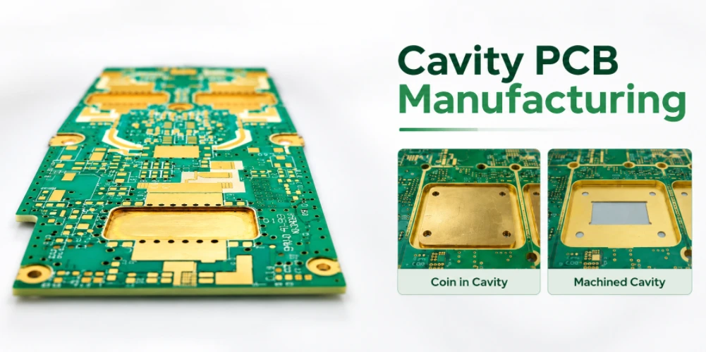
OEM-tuotteiden erikoispiirteiset piirilevyt
Highleap Electronics / PCB + PCBA...
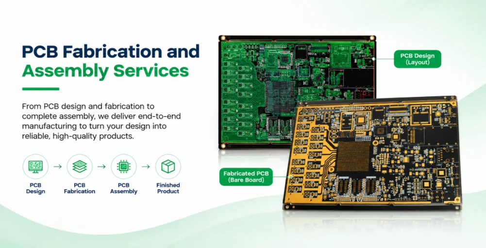
Piirilevyjen valmistus- ja kokoonpanopalvelut
Highleap Electronics tarjoaa piirilevyjen valmistusta ja kokoonpanoa...
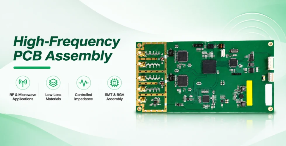
Korkean taajuuden piirilevyjen kokoonpanopalvelut
Highleap Electronics tarjoaa korkeataajuista piirilevyjen kokoonpanoa...
Miten saada tarjous piirilevyistä
Suoritetaan DFM/DFA-analyysi puolestasi ja lähetetään sinulle raportti. Voit ladata tiedostosi turvallisesti verkkosivustomme kautta. Tarvitsemme seuraavat tiedot voidaksemme antaa sinulle tarjouksen:
-
- Gerber, ODB++ tai .pcb, sp.
- Tuoteluettelo, jos tarvitset kokoonpanoa
- Määrä
- Käännä aika
Piirilevyjen valmistuksen lisäksi tarjoamme kattavan valikoiman elektroniikkapalveluita, kuten piirilevysuunnittelua, piirilevyasennusta ja kokonaisratkaisuja. Tarvitsetpa apua prototyyppien valmistuksessa, suunnittelun varmentamisessa, komponenttien hankinnassa tai massatuotannossa, tarjoamme kokonaisvaltaista tukea projektisi onnistumisen varmistamiseksi.
Piirilevypalveluita varten toimitathan osaluettelosi (BOM) ja mahdolliset erityiset kokoonpano-ohjeet. Tarjoamme myös DFM/DFA-analyysin suunnitelmiesi valmistettavuuden ja kokoonpanon optimoimiseksi varmistaen sujuvan tuotantoprosessin.