
KB-6168LE PCB: Przewodnik po produkcji i montażu cienkowarstwowych płytek wielowarstwowych
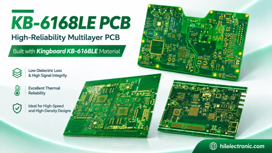

Looking for a PCB factory to manufacture a thin multilayer board with Kingboard KB-6168LE? Highleap Electronics provides multilayer PCB fabrication and PCB assembly based on customer-approved material specifications and production files. We manufacture the finished PCB and PCBA; we do not manufacture the KB-6168LE laminate itself.
For this material-specific build, the important question is whether the specified construction can be translated into a stable, manufacturable board. Highleap reviews the material requirement together with the stackup, finished thickness, copper structure, drilling details and assembly needs—so you can clarify the build before committing to production.
KB-6168LE PCB Manufacturing: From Material Requirement to Finished Board
When KB-6168LE is specified on a drawing or material list, you need a PCB manufacturer that can work to that requirement—not a supplier that simply offers a similar-looking FR-4 alternative. Highleap’s role is to manufacture the board to the approved construction and keep the material requirement connected to the fabrication documentation.
For a KB-6168LE project, our manufacturing review focuses on the details that determine whether the board can be built as designed:
- Material and sourcing: Confirm the required KB-6168LE construction and whether the material will be customer-supplied or needs to be sourced.
- Stackup and thickness: Review the layer sequence, dielectric build, copper weights and finished board thickness.
- Wymagania dotyczące produkcji: Check registration, lamination, drilling, plating, finishing and dimensional requirements against the supplied files.
- Zakres montażu: Confirm whether you need bare PCBs only or finished PCB assemblies as well.
Highleap supports multilayer PCB fabrication from prototype requirements through production orders, with the actual process and feasibility confirmed against the final layer count, thickness, tolerances and via structure. If you are comparing material-specific builds, our Usługa materiałów laminowanych PCB explains how customer-specified materials are coordinated with PCB construction and production.
KB-6168LE Material Supply and Build Confirmation
One of the first quotation questions is whether the exact KB-6168LE material construction is available for the project. Highleap is a PCB and PCBA manufacturer, not the laminate producer. We can review a customer-specified material requirement and coordinate sourcing as part of the PCB project where supply can be confirmed. If you already have the material, tell us whether it will be supplied by your team.
To avoid an incorrect substitution or an incomplete quotation, please identify:
- The exact KB-6168LE material designation and the current Kingboard specification you are working to.
- The approved laminate and bonding-layer construction for the proposed layer build.
- Whether the material is customer-supplied or needs to be sourced.
- Whether alternative materials are prohibited or may be considered only with written approval.
The public UL information lists KB-6168LE as an FR-4.0 ultrathin industrial laminate for multilayer printed wiring boards, with specific minimum build-up thickness conditions. Those entries must be read as construction-specific recognition information, not as a universal finished-board thickness range. For production, the customer’s current Kingboard documentation and the applicable recognized construction take precedence.
Thin Multilayer Stackup and Lamination for KB-6168LE PCB
For an ultrathin multilayer PCB, the stackup is not just a drawing attachment. It is the manufacturing definition for how the specified material, dielectric layers and copper are combined into the finished board. If the material callout, pressed dielectric thickness and finished board thickness do not agree, the project can run into avoidable engineering and quotation delays.
Send Highleap the complete stackup so we can review:
- Total layer count and exact layer sequence.
- KB-6168LE material identification and dielectric construction by layer.
- Pressed dielectric thicknesses and finished board thickness with tolerance.
- Inner- and outer-layer copper weights and copper distribution.
- Reference planes, critical signal layers and impedance requirements, if applicable.
- Via structure, drill sizes, finished-hole requirements and panelization constraints.
Nasza Inżynieria układania warstw PCB oraz Laminowanie PCB services are relevant at this stage. Reviewing the construction before tooling helps establish whether the proposed layer build, pressing plan and finished thickness are consistent with the customer’s requirements.
KB-6168LE PCB Fabrication and Process Control
Once the material and stackup are confirmed, the next step is to translate the released design into a controlled fabrication route. For a thin multilayer build, the critical points are usually the interaction between registration, lamination, board handling, drilling, plating and final dimensions—not the material name by itself.
- DFM and tooling review: Check clearances, annular rings, drill data, layer alignment and drawing consistency before production tooling.
- Lamination and registration: Follow the approved material sequence and review the requirements for pressed thickness and layer-to-layer alignment.
- Wiercenie i powlekanie: Set the process requirements according to finished thickness, hole size, aspect ratio and interlayer connection design.
- Wykończenie i kontrola: Confirm solder mask, surface finish, dimensional inspection and electrical testing requirements.
Highleap's Recenzja PCB DFM helps identify manufacturing issues in the supplied design before release. Our Proces produkcji PCB covers the production stages from inner-layer processing and lamination through drilling, plating, finishing and electrical testing. For the KB-6168LE build, the process is finalized against the approved files and confirmed production requirements.
KB-6168LE PCB Assembly and Turnkey PCBA
If your project requires assembled boards, Highleap can continue from PCB fabrication into SMT or THT assembly, inspection and testing. Keeping the bare-board and assembly requirements in the same quotation review helps ensure that the board construction, panel design and assembly documentation are considered together.
For a PCBA quotation, provide the BOM, pick-and-place file, assembly drawings, component orientation details and any special inspection or functional-test requirements. For thin boards, also identify any panel rails, tooling holes, fiducials or support requirements needed for handling during assembly.
Highleap zapewnia Usługi montażu PCB oraz Montaż PCB pod klucz for customers who want to combine bare-board fabrication with component sourcing and assembly. You can request a bare PCB quotation or submit the complete assembly package for a combined PCBA review.
Get a KB-6168LE PCB Manufacturing Quote
To quote the actual build—not just the material name—send the following information. If a detail is not finalized, mark it as open so the engineering team can identify what needs confirmation.
- Pliki produkcyjne: Gerber or ODB++ data, NC drill files and fabrication drawing.
- Wymagania materiałowe: KB-6168LE designation, current Kingboard documentation and approved construction.
- Stos: Layer count, layer sequence, dielectric thicknesses, copper weights and finished board thickness/tolerance.
- Manufacturing notes: Via structure, drill requirements, surface finish, solder mask and dimensional tolerances.
- Wymagania elektryczne: Controlled impedance, test coupons and electrical test criteria, if applicable.
- Szczegóły zamówienia: Quantity, prototype or production stage and required delivery schedule.
- Dostawa materiałów: Whether KB-6168LE will be customer-supplied or needs sourcing.
- Pliki PCBA: BOM, pick-and-place data and assembly drawings, if assembly is required.
Thin Multilayer PCB Fabrication · PCB Assembly
Have a KB-6168LE PCB Build to Quote?
Send your stackup, material specification, fabrication files and quantity. Highleap will review the required construction and manufacturing scope for your bare PCB or complete PCBA project.

Polecamy Wiadomości
Produkcja płytek PCB TMM
Spis treści Zakres produkcji płytek PCB TMM dla RF i...

Wycena i zestawienie PCB RT duroid 6002
Ta strona zawiera zadanie wyceny i definicji stosu...
Produkcja płytek PCB filtrów TMM6
Spis treściDlaczego projektanci filtrów mikrofalowych używają...
Taconic RF 35 vs RO4350B PCB
Spis treściRF-35 vs RO4350B Zaopatrzenie i...
Jak uzyskać wycenę płytek PCB
Przeprowadzimy dla Ciebie analizę DFM/DFA i prześlemy raport. Możesz bezpiecznie przesłać pliki za pośrednictwem naszej strony internetowej. Aby przygotować wycenę, potrzebujemy następujących informacji:
-
- Gerber, ODB++ lub .pcb, specyfikacja.
- Lista BOM, jeśli wymagany jest montaż
- Ilość
- Czas na zmianę
W przypadku usług PCBA prosimy o dostarczenie BOM (listy materiałów) i wszelkich szczegółowych instrukcji montażu. Oferujemy również analizę DFM/DFA w celu optymalizacji projektów pod kątem możliwości produkcji i montażu, zapewniając płynny proces produkcji.