
Изготовление печатных плат Arlon 45NK с низким коэффициентом теплового расширения в Китае.
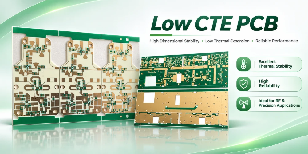
Иллюстрация процесса изготовления печатной платы. Подтвердите указанный класс материала Arlon в проектной документации и системе отслеживания материалов.
Arlon 45NK PCB design is about controlling expansion mismatch at the solder-joint interface, while preserving manufacturable multilayer geometry. It is a woven-aramid-reinforced epoxy laminate/prepreg system, not a ceramic substrate and not a high-temperature polyimide. Its low in-plane coefficient of thermal expansion (CTE) makes it relevant when a leadless ceramic chip carrier or another low-expansion package is mounted on a PCB that undergoes repeated temperature changes.
For Highleap Electronics, this is a problem that spans bare-board manufacturing and PCBA: laminate architecture and dimensional control affect pad registration, while assembly profile, footprint and thermal cycling affect joint reliability. Material sourcing and the actual fabrication/assembly route still need to be verified for a particular order. An Arlon 45NK low-CTE PCB manufacturing enquiry is most useful when it includes the ceramic-package geometry and assembly thermal-cycle profile, not just the laminate name.
Arlon 45NK PCB — At a Glance
The low X/Y CTE targets low-expansion component interfaces. Arlon also lists 2.8% Z-axis expansion over its referenced range and 0.80% water absorption; the axes and tests must not be conflated.
The Engineering Problem: Board-to-Package Expansion Mismatch
A ceramic package and the PCB beneath it do not necessarily grow by the same amount during heating. That difference creates relative motion across solder joints. The concern is especially important for leadless parts whose joints have little geometric compliance. Choosing a low-CTE laminate can reduce this один компонент of strain, but component size, stand-off, pad layout, solder alloy and thermal-cycle duration remain significant.
Arlon identifies 45NK as woven aramid reinforced multifunctional epoxy, with published X/Y CTE about 5–7 частей на миллион/°C, Tg approximately 170 ° C и UL 94 V-0. Its purpose is not simply to be a ‘stronger FR-4.’ The reinforcement architecture changes in-plane expansion and also changes how a panel behaves under pressing, cutting and drilling. That trade-off needs to be understood before a design is released.
A simple displacement calculation, with its limitations
Рассмотрим hypothetical 30 mm long ceramic package with an assumed expansion coefficient of 7 ppm / ° C и 100 ° C temperature change. For comparison, suppose a conventional glass-reinforced board construction has 17 ppm/°C in-plane CTE. The difference in free thermal expansion along the 30 mm distance is:
ΔL = (αboard − αpackage) × L × ΔT = (17 − 7) × 10⁻⁶/K × 30 mm × 100 K = 0.030 mm = 30 µm.
If a 45NK-based construction behaves at 6 ppm/°C under the same assumptions, the corresponding free-expansion difference is (6 − 7) × 10⁻⁶ × 30 × 100 = −0.003 mm, Или о 3 µm in magnitude. This is an illustration of mismatch displacement, not a prediction of solder-joint fatigue life. A real assembly has a temperature-dependent package stiffness, local copper effects, solder viscoplasticity, constraints and gradients. Its joints must be assessed using the actual product geometry and cycling profile.
Distance-to-neutral-point (DNP) clarification: The 30 mm dimension in the calculation above represents the full package span; its 30 µm and 3 µm results are end-to-end free-expansion differences. For a symmetric package with its neutral point at the center, a hypothetical edge joint at DNP = 15 mm instead has an idealized local mismatch magnitude of 15 мкм on the 17 ppm/°C board and 1.5 мкм on the 6 ppm/°C construction for the same 100°C change.
Local screening relation: |Δu| ≈ |αПечатные платы - αпакет| × DNP × |ΔT|. The result is free relative displacement—not solder shear strain or validated fatigue life. Joint restraint, package bending, the neutral-point location and actual temperature gradients can change the result.
Idealized mismatch over a 30 mm span (illustration only)
Таблица: на узких экранах проведите пальцем по горизонтали, чтобы просмотреть все столбцы.
| Технология | Why it changes the design decision |
|---|---|
| Package CTE and body size | Determine the free-expansion mismatch and distance from the neutral point |
| Board X/Y CTE | Sets the substrate contribution; copper and lay-up influence the effective value |
| Solder stand-off and joint geometry | Determine how relative motion is accommodated |
| Operating temperature range and dwell | Influence cyclic strain and creep, not just peak temperature |
| Mounting fixtures, stiffeners and connectors | Can restrict free movement and create local stress concentrations |
A good material recommendation begins by locating the actual vulnerable component interface. For some products, package redesign, pad changes, stand-off or thermal management may be more effective than changing the entire substrate. For others, the use of low-expansion PCB materials is a central part of the reliability argument.
Material trade-offs beyond X/Y expansion
Arlon’s controlled-expansion product table also lists 2.8% Z-axis expansion и 0.80% водопоглощение for 45NK. These are separate material tests, not evidence that a given finished stack-up will have 2.8% through-thickness growth or that its assembly is unsuitable for humidity. They do mean that low X/Y CTE should not be generalized to all axes or all environmental risks. Check the reinforcement orientation, prepreg storage, board thickness, moisture controls and plated-hole geometry when designing the complete board.
Low-CTE Stack-Ups Must Still Be Electrically and Mechanically Buildable
Once the target expansion behavior is understood, the PCB must still satisfy trace geometry, layer registration and insulation requirements. The measured laminate CTE is not automatically the effective CTE of an assembled stack-up with copper-heavy planes on one side, sparse signal layers on the other and local attachments. An imbalanced construction may bow during processing and change solder-paste transfer or component seating even if the nominal material CTE is low.
Tie the component interface to the board design
- Start at the package: identify leadless ceramic packages and other rigid components, their footprint, joint geometry, local copper thermal mass and expected temperature profile.
- Set the required stack-up: specify 45NK core/prepreg construction, copper weights, dielectric thicknesses and any critical impedance targets. The laminate does not exempt high-speed nets from electrical verification.
- Control construction symmetry: consider copper distribution and laminate balance to manage bow/twist; coordinate panel layout and fiducials with the assembly route.
- Define tolerances at the right location: a global finished-board dimension alone may not be sufficient if the risk is local pad-to-pad registration beneath a large leadless package.
- Choose an acceptance method: evaluate dimensional measurements, warp/bow and assembled first articles against product drawings rather than assuming that a low-CTE number guarantees SMT yield.
For multilayer designs, an accurate Наложение слоев печатной платы should connect substrate thickness, plated-hole requirements, copper distribution and controlled impedance to the physical assembly. If a change in copper weight improves thermal spreading but alters local board stiffness or effective CTE, the mechanical and electrical consequences should be reviewed together.
Woven Aramid Changes the Lamination and Machining Process
This is the part that generic low-CTE articles often miss. Arlon’s own process notes state that aramid fabric compresses and distorts under pressure more readily than E-glass. The low-expansion reinforcement can therefore introduce a fabrication-specific risk: a press setup developed for conventional glass-cloth laminates may create unnecessary fabric movement or registration error. Simply substituting an aramid material into a familiar FR-4 traveler is not a controlled process.
What the supplier recommends—and what a fabricator must still validate
Arlon’s published 45NK information includes a 30-minute pre-vacuum, a controlled heat rise of about 4.5–6.5°C/min between 100°C and 150°C, a cure point around 180°C held for 90 minutes, and cooling under pressure at no more than 5 ° С / мин. It also recommends inner-layer preparation and conditioning before lay-up. These are material-supplier reference conditions; the actual process window depends on lay-up, panel dimensions and the production press.
The supplier illustrates how vacuum-assisted pressing can permit substantially lower pressure than a non-vacuum approach. This is not an instruction to apply a single pressure to every 45NK panel. The fabricator must confirm compaction, resin flow, void content, dielectric thickness and dimensional stability using its own panel construction. Press pressure that is too low can leave voids or inadequate bond formation; pressure that unnecessarily distorts the textile can undermine registration. Both outcomes are unacceptable even if the board meets its nominal finished thickness.
Material-document control: Arlon’s 45NK product webpage states IPC-4101/50 with material type AFN, while its 45NK PDF lists IPC-4101/50 with type AFG. Because these supplier documents do not agree on that identifier, the released OEM drawing should use a customer-approved designation and obtain current written clarification before specifying a type code. Do not infer an equivalent type from the resin name alone.
Also verify any pressure-unit conversion before using old printed process examples: 300 psi is approximately 21.1 kgf/cm², not 2 kgf/cm². Panel-specific press pressures still require qualification.
Practical first-panel checks
Таблица: на узких экранах проведите пальцем по горизонтали, чтобы просмотреть все столбцы.
| Этап производства | Что следует контролировать | Evidence worth collecting |
|---|---|---|
| Обработка материалов | Moisture exposure, prepreg conditioning, reinforcement identity | Material records and recorded pre-lay-up preparation |
| расслоение | Press cycle, resin fill, cloth compression and movement | Coupon thickness, registration measurements and cross-sections |
| Сверление и фрезеровка | Fiber pull-out, fuzzy edges, hole-wall quality, tool wear | Hole-wall inspection and representative routed-edge checks |
| Медная обшивка | Through-hole integrity after aramid drilling | Plating acceptance and cross-sections where required |
| Заключительная панель | Bow/twist and dimensional repeatability | Defined panel/board measurements before SMT |
Woven aramid can also demand attention during mechanical finishing. Fiber pull-out and edge quality are not solved by a material datasheet alone. Drill tools, entry/backing support and routing parameters should be validated against the required hole geometry and edge specification. Highleap’s Изготовление печатных плат review needs to establish those acceptance requirements before the first production release.
Connect Fabrication Evidence to SMT Solder-Joint Reliability
The point of choosing 45NK is often at the component interface, so the finished article cannot be judged solely as a bare board. A panel that meets electrical test can still have local bow that complicates paste printing; a solder joint that passes AOI can still be vulnerable to fatigue under the product’s field temperature cycles.
An evidence plan across the two manufacturing stages
- Bare board: verify material construction, geometry, flatness, hole quality and the copper stack-up. Record any departures that change the intended effective CTE.
- Настройка сборки: confirm paste, stencil apertures, placement support and reflow conditions appropriate to the selected leadless package. A heavier copper plane can create local thermal differences even when the laminate itself is suitable.
- Первоначальный осмотр: use visual/AOI methods for accessible features; X-ray or other techniques may be needed for concealed joints, depending on the package.
- Квалификация надежности: define the product’s thermal-cycle limits, dwell, sample size and pass criteria with the OEM. Electrical monitoring and post-test failure analysis can be more meaningful than merely counting visible cracks.
- Изменить контроль: if the package, pad geometry, solder alloy or PCB construction changes, evaluate whether the previous assembly qualification remains applicable.
The same OEM may order only bare boards or a complete SMT-assembled PCBA. The value of coordinating both is that a materials decision can be evaluated against soldering and inspection requirements before the design and process are frozen. That does not mean Highleap can warrant a fatigue lifetime without an agreed qualification program.
Arlon 45NK Low-CTE PCB Manufacturing: Selection and RFQ
45NK can be appropriate when a low-expansion package creates a genuine board/package mismatch problem and the added material and process requirements are justified. It is less persuasive if the product’s dominant risk is heat dissipation through a metal chassis, a connector’s mechanical load or a solder-joint geometry problem unrelated to board CTE. A material with a Tg of 170°C also should not be described as a substitute for a 250°C polyimide merely because both may be used in demanding electronics.
For an actionable quote, send the released fabrication files, board dimensions, layer stack-up and copper weights; 45NK core/prepreg callout; relevant impedance requirements; critical package drawings and footprint information; warp/flatness criteria; assembly drawings, BOM, solder alloy and reflow constraints; expected operating temperature cycle; and any required thermal-cycling tests. If the PCB will be supplied without assembly, specify the controls the assembler must receive or inspect.
Highleap can review the requested Производство печатных плат и сборка печатных плат scope, material availability, geometry and proposed acceptance package. The goal is a buildable board and a defined interface to SMT—not an unsupported statement that a low-CTE laminate alone solves every solder-joint problem.
Selecting an Arlon 45NK Low-CTE PCB Manufacturer for Ceramic Packages
An Arlon 45NK PCB manufacturer must review more than the nominal in-plane CTE. For a rigid leadless ceramic package, the relevant design includes the package CTE, distance from the neutral point, solder-joint geometry, local copper distribution, board constraint and expected thermal cycles. These are the inputs that connect low-CTE PCB fabrication to an assembly-level reliability argument.
What to send with a 45NK PCB fabrication request
Supply the stack-up, critical package dimensions, pad geometry, assembly drawing, thermal-cycle assumptions, copper weights and finished-board flatness or registration requirements. When available, include a preliminary package-to-board mismatch assessment rather than treating the published 45NK X/Y CTE as the effective CTE of every finished stack-up. A sourcing discussion should also include aramid-related drilling, routing, moisture and edge-quality controls.
Low-CTE board sourcing for US and Canadian design teams
Для инженеров в США или Канада comparing domestic and overseas PCB fabrication options, the practical question is whether the build specification preserves the intended package interface. Confirm the agreed units, drawing revision, first-article measurements, SMT handoff and the parties responsible for thermal-cycle evaluation. The same technical requirements apply wherever a board is fabricated; regional location does not itself establish the suitability of a material for a ceramic carrier.
Highleap is a China-based PCB fabrication and assembly supplier and can assess an Arlon 45NK PCB manufacturing enquiry against the supplied design. Arlon 45NK material availability, woven-aramid processing and any Arlon 45NK PCB assembly scope require order-specific review. The goal is a traceable feasibility decision, not an unsupported claim that a low-CTE laminate guarantees a particular solder-joint life.
Arlon 45NK PCB — Frequently Asked Questions
Does low in-plane CTE guarantee a longer solder-joint life?
No. It can reduce free-expansion mismatch with a compatible package, but fatigue depends on distance from the neutral point, board restraint, joint height, solder alloy, dwell time, gradients and the actual thermal-cycle profile.
Is Arlon 45NK a polyimide material?
No. Arlon identifies 45NK as a woven-aramid-reinforced multifunctional epoxy laminate and prepreg. Its process and CTE tradeoffs differ from high-temperature polyimide grades such as 33N or 86HP.
What is special about drilling and laminating woven aramid?
The reinforcing textile can distort under excessive press pressure, and mechanical processing can create fiber pull-out or fuzzy edges. Tooling, pressure, vacuum assistance, registration and first-panel inspection must be validated for the actual design.
What information helps a supplier review an Arlon 45NK low-CTE PCB for a ceramic package?
Include the layer stack-up, package and pad geometry, distance from the neutral point where relevant, estimated package CTE, temperature-cycling profile, copper distribution, flatness or registration limits and SMT constraints. Confirm the material and fabrication route separately; published in-plane CTE alone cannot establish assembled solder-joint life.
Have a PCB design specifying Arlon 45NK? Компания Highleap Electronics может оценить файлы печатной платы, структуру слоев, требования к материалам, производственные ограничения и, при необходимости, объем сборки печатной платы. Укажите количество вашего заказа и критерии приемки, чтобы в коммерческом предложении учитывались фактические требования к изготовлению.
Технические условия и границы испытаний: указанные выше значения Arlon представляют собой опубликованные данные о материалах или иллюстративные рекомендации поставщика по технологическим процессам, а не результаты производства Highleap, гарантированную возможность сборки печатных плат или квалификацию продукции. Подтвердите версию, форму материала, применимую спецификацию IPC, наличие партии и план приемки для каждого проекта.
Технические справочные материалы: Arlon 45NK product and process information; Controlled thermal expansion product family.
45NK manufacturer PDF (for IPC-4101/50 type-label cross-check).

Об авторе
Хелен Чонг
Консультант по решениям для печатных плат и менеджер по развитию зарубежного бизнеса в компании Highleap Electronics.
Хелен оказывает поддержку международным инженерным командам, предоставляя комплексные решения по изготовлению и сборке печатных плат, помогая проектам переходить от быстрого создания прототипов к стабильному серийному производству. Ее опыт охватывает высокочастотные и радиочастотные платы, сложные многослойные структуры, технологии жестко-гибких и гибких печатных плат в различных отраслях.
Переводя технические требования в практические планы производства, она помогает клиентам улучшить технологичность, снизить риски, оптимизировать затраты и сроки выполнения заказов, сохраняя при этом стабильное качество в больших масштабах.

Рекомендуемые сообщения
Изготовление и сборка многослойных печатных плат KB-6165LE
HIGHLEAP ELECTRONICS / KB-6165LE / Многослойная печатная плата...
KB-6165GC Производство печатных плат и сборка печатных плат
HIGHLEAP ELECTRONICS / KB-6165GC / БЕЗГАЛОГЕННАЯ ПЕЧАТЬ...
Производитель печатных плат KB-6165C для силовых и контрольных плат.
HIGHLEAP ELECTRONICS / KB-6165C / Плата питания и управления...

Китайский производитель печатных плат с 14-слойным толстым слоем меди для сильноточных плат
СИЛЬНОТОКОВАЯ / СМЕШАННАЯ МЕДЬ · ВЫСОКИЙ СПРЫСОК...
Как получить расценки на печатные платы
Давайте проведем для вас анализ DFM/DFA и вернемся к вам с отчетом. Вы можете безопасно загрузить свои файлы через наш веб-сайт. Для того, чтобы дать вам предложение, нам нужна следующая информация:
-
- Gerber, ODB++ или .pcb, спец.
- Список спецификаций, если вам требуется сборка
- Количество
- Время поворота
Помимо производства печатных плат, мы предлагаем широкий спектр электронных услуг, включая проектирование печатных плат, печатные платы и готовые решения. Если вам нужна помощь с прототипированием, проверкой дизайна, поиском компонентов или массовым производством, мы оказываем комплексную поддержку, чтобы гарантировать успех вашего проекта.
Для услуг PCBA, пожалуйста, предоставьте ваш BOM (спецификация материалов) и любые конкретные инструкции по сборке. Мы также предлагаем анализ DFM/DFA для оптимизации ваших проектов для технологичности и сборки, обеспечивая плавный процесс производства.