
Hard Gold Finger PCB Manufacturing: Plating and Beveling
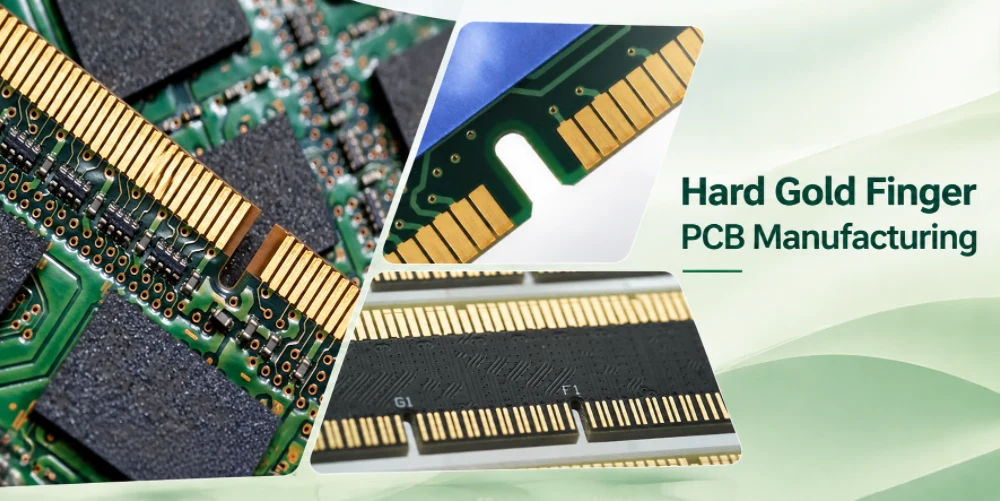
Hard gold finger PCB manufacturing is used when a circuit board needs exposed edge contacts designed for repeated mating with a connector. The manufacturing specification must define more than a gold-colored surface: it must identify the contact area, plating construction, finished board thickness, edge geometry and inspection criteria that determine whether the board fits and performs as intended.
For PCB buyers, a common risk is sending a supplier a Gerber package with a note such as “gold fingers” but no complete plating or bevel specification. That leaves key decisions open to interpretation and makes quotations difficult to compare. A board may look acceptable while still having the wrong finish, insufficient contact length after beveling, or dimensions that do not match the mating connector.
Highleap Electronics manufactures PCBs and provides PCB assembly services. For hard gold finger projects, the practical starting point is a controlled review of the customer’s fabrication data, mechanical drawing, contact requirements and order scope. The purpose is to resolve manufacturing questions before release—not to assume a universal plating thickness, bevel angle or tolerance for every design.
Содержание
- 1. Define Hard Gold Finger PCB Requirements Before Quotation
- 2. Specify Selective Hard Gold Plating and Distinguish ENIG
- 3. Control Gold Finger Geometry and Beveling
- 4. Review CAM Data, Panelization and Fabrication
- 5. Define Inspection and Compare Manufacturing Cost
- 6. Prepare a Production-Ready RFQ for Hard Gold Finger PCBs
HARD GOLD FINGER PCB
Need a Hard Gold Finger PCB Quote?
Send the PCB files, plating specification, connector drawing, bevel details and order quantity for a project-specific review.
Запросить ценовое предложение на печатную плату →1. Define Hard Gold Finger PCB Requirements Before Quotation
The phrase “hard gold finger PCB” describes the intended contact feature, but it does not fully define the board. Before a supplier can quote the job accurately, the design package should identify the connector interface and the characteristics that affect contact fit, plating and manufacturing acceptance.
| Указанный пункт | What the manufacturer needs to know | Почему это важно |
|---|---|---|
| изготовление печатных плат | Layer count, laminate, copper weight, stackup and finished thickness | Sets the board structure and the dimensional basis for connector fit |
| Finger geometry | Finger width, pitch, length, spacing and position from the board datum | Controls alignment with the mating connector |
| Контактный финиш | Hard gold and nickel requirements, specified thicknesses and acceptance limits | Defines the contact plating system rather than a generic gold appearance |
| Обработка кромок | Bevel angle, depth or remaining edge thickness, and tolerances where required | Determines the insertion profile and usable contact area |
| Схема платы | Finished dimensions, critical datums, slots and cutouts | Helps prevent interference with the connector or housing |
| Требования к качеству | Dimensional checks, plating verification, electrical testing and reports | Establishes how the delivered boards will be accepted |
| Информация о заказе | Prototype or production quantity, delivery target and packing requirements | Allows the supplier to quote the intended commercial scope |
These requirements interact. A change to finished board thickness can affect connector engagement. A longer bevel can reduce the remaining contact length. A plating note that does not identify the required region can lead to different interpretations of which surfaces receive hard gold.
Provide the connector manufacturer’s drawing or an approved interface drawing whenever possible. If the connector has a permitted PCB thickness range, critical contact dimensions or a specified insertion profile, those requirements should inform the PCB drawing. Do not rely on dimensions copied from a visually similar board unless the design owner has approved them.
Highleap gold finger PCB manufacturing overview provides related context for the contact structure. For quotation and production release, however, the controlled project drawing and customer specification remain the governing documents.
2. Specify Selective Hard Gold Plating and Distinguish ENIG
Hard gold fingers are typically produced using electroplated gold over a nickel underplate, according to the customer’s specified construction. The nickel layer serves as a barrier between the copper and the gold finish, while the hard gold deposit is selected for the intended contact and wear requirements. The exact deposit requirements must come from the connector specification, product reliability targets or other approved customer documentation.
What the plating note should include
- Plating area: Mark the fingers or other contact surfaces that require hard gold, and identify areas that must not receive this finish.
- Толщина золота: State the required value or range, units, applicable minimums and the acceptance basis.
- Nickel underplate: Define the required nickel specification and thickness where controlled by the design.
- Метод проверки: State whether thickness measurements or a report are required, including any sampling or location requirements.
- Применимый стандарт: Reference the customer’s approved specification or standard and its revision where relevant.
Do not select a gold thickness solely because it is commonly quoted by another supplier. Required thickness can depend on the connector, expected mating cycles, contact loading, environment and customer acceptance criteria. A thicker deposit can increase cost and does not automatically compensate for incorrect contact geometry or poor connector alignment.
Hard gold and ENIG are different finish requirements
Electroless nickel immersion gold (ENIG) is commonly used on solderable component pads. Electroplated hard gold is commonly specified for edge contacts that need to meet a defined wear requirement. The two finishes are not interchangeable simply because both appear gold-colored. A board may require hard gold on its fingers and a different finish on component pads; the fabrication drawing should make the finish regions clear.
For a side-by-side explanation of the two options, see Highleap’s guide to ENIG versus hard gold PCB finishes. For production, the supplier still needs the project’s actual finish callouts and approved acceptance limits.
3. Control Gold Finger Geometry and Beveling
The contact fingers must align with the mating connector, and the finished board edge must enter the connector without unintended interference. Finger width, pitch, length, finished board thickness and outline tolerances should therefore be reviewed as one mechanical interface rather than as independent artwork values.
Check finger dimensions against the connector
Finger width and pitch influence contact alignment and electrical isolation. Contact length affects the available engagement area, while board thickness influences the fit inside the connector slot. The drawing should identify critical dimensions and their reference datums so the fabricator can inspect the same features that the design owner considers functionally important.
The exposed contact region also needs a clear boundary. Solder mask, legend ink or other coatings should not encroach on the required contact surface. Vias, pads, slots and nearby copper must be checked against the contact layout and the mechanical profile.
Specify the bevel instead of assuming a default
Beveling creates a lead-in at the board edge for applications where the PCB slides into a card-edge connector. The required angle and depth depend on the connector and the mechanical design; no single angle or depth is appropriate for every board. A useful drawing specifies the angle, the edge to be machined, the bevel depth or remaining edge thickness, the finished board thickness and any applicable tolerances.
Because beveling removes material, the design must account for the contact length that remains after machining. Internal copper near the beveled edge also requires review: if copper extends into the material-removal zone, machining may expose copper that was not intended to be a contact surface. This is especially important on multilayer boards, where the internal copper geometry cannot be judged from the top-layer image alone.
Consider plating access and panel layout
Electroplating needs an electrical path to the areas being plated. Depending on the panel and contact design, temporary plating connections or bus structures may be required. Their location, connection and removal or separation must be considered during CAM preparation and panelization. If the supplied data does not show a workable plating approach, the manufacturer should raise the question before production rather than make an undocumented change.
Highleap reviews the supplied artwork and mechanical notes to identify these kinds of design-to-process conflicts. Any proposed change to finger geometry, beveling or the plating route should be approved by the customer when it affects the released design or acceptance requirements.
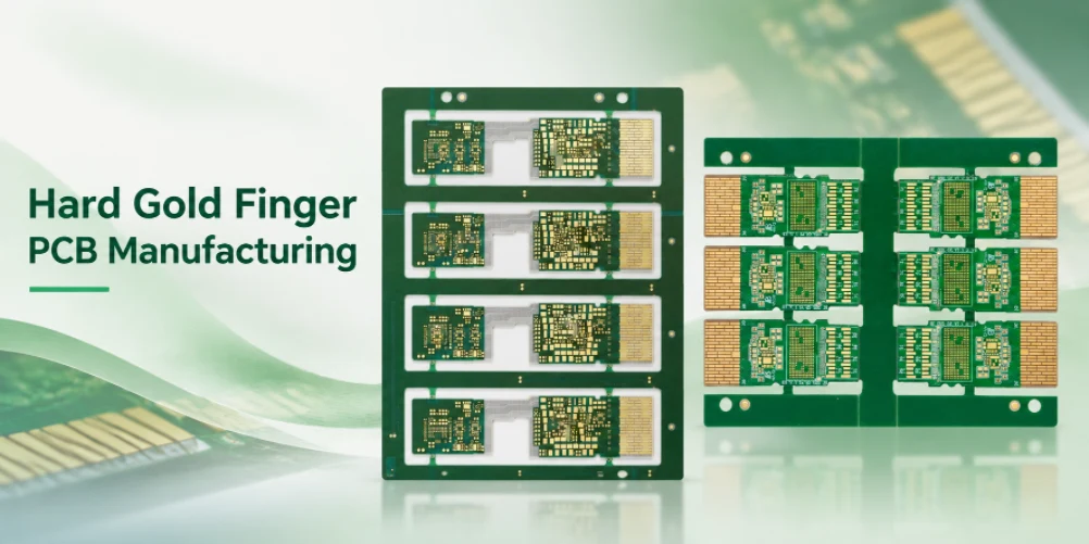
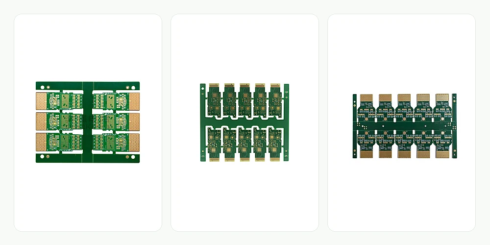
Panelized hard gold finger PCBs with connector contacts
4. Review CAM Data, Panelization and Fabrication
A CAM review should confirm that the fabrication files, mechanical drawing and manufacturing notes describe the same finished PCB. Opening the Gerber files is only the first step. The review should reconcile the board outline, drill data, layer structure, finish regions, thickness, bevel requirements and any customer-specific instructions before the production data is released.
CAM checks for hard gold finger boards
- Revision matching: Confirm that Gerber or ODB++ data, NC drill files, stackup, fabrication drawing and purchase-order references identify the same approved revision.
- Outline and datum consistency: Compare the copper and outline data with the dimensioned drawing, including slots, cutouts and contact position.
- Plating definition: Confirm the intended hard gold region, nickel/gold requirements and any other finish regions.
- Bevel compatibility: Review the edge profile against finished thickness, contact length and nearby copper.
- Drill and clearance review: Check hole definitions and relevant copper clearances against the drawing and the proposed edge machining.
- Открытые вопросы: Document conflicting or missing instructions and obtain clarification before production release.
For example, if the fabrication drawing specifies a bevel but the board outline or contact drawing does not identify the reference edge, the supplier should ask for clarification. If a plating note conflicts with the finish callout, the discrepancy should be resolved before the process route is fixed. An ambiguous specification should not be silently converted into an assumed requirement.
Panelization must support both fabrication and delivery
The production panel should provide a workable arrangement for plating, handling, machining and separation while maintaining the required contact geometry. The review should consider the number and orientation of boards, process rails or tooling features where needed, the location of the gold finger edges, the separation method and the final delivered quantity. The best panel is not necessarily the one that fits the most circuits on a raw sheet if it makes plating access, edge processing or safe handling more difficult.
If the boards will subsequently be assembled, the panel format should also be checked against the assembly process. The bare-board panel and the assembly array may have different requirements, but the transition between them needs to be agreed. Highleap’s Услуги по изготовлению печатных плат covers the broader board-manufacturing scope; the specific gold finger process route is confirmed from each project’s approved files and requirements.
Keep manufacturing changes under revision control
Changes to laminate, copper layout, plating, bevel geometry or board thickness can affect fit or acceptance even if the board looks similar. If a manufacturing adjustment is needed, record the issue, proposed solution and customer approval in the project’s revision-controlled documentation. This is especially important for repeat orders and second-source manufacturing.
5. Define Inspection and Compare Manufacturing Cost
Hard gold finger PCB quality needs to be judged against the characteristics that control contact fit and function. A bright surface is not enough, and a standard electrical continuity test does not by itself verify plating thickness, bevel geometry or connector insertion performance. The inspection plan should state what is measured, how it is measured and which acceptance criteria apply.
Match inspection to the drawing
- Проверка покрытия: If gold or nickel thickness is a controlled characteristic, specify the measurement method, locations or sampling plan and reporting requirement. X-ray fluorescence (XRF) is one method commonly used for coating-thickness measurement when suitable for the specified coating system.
- Проверка размеров: Check the critical finger dimensions, board thickness, outline and bevel geometry against the approved drawing.
- Surface and edge condition: Define acceptance for scratches, contamination, peeling, uneven deposits, machining damage and unintended copper exposure.
- Электрический тест: Specify the required bare-board open/short test and any additional electrical verification.
- Application qualification: If the end product requires contact-resistance limits, insertion-cycle testing or environmental qualification, identify those requirements separately. They are not automatically covered by ordinary PCB inspection.
What drives hard gold finger PCB cost?
Quotation depends on the full board specification rather than a single “gold finger” feature. Relevant cost factors include board construction and layer count, laminate and copper requirements, plating area and deposit specification, beveling, tight dimensional tolerances, panel utilization, order quantity and the inspection records requested.
| Коэффициент котировки | Questions to compare across suppliers |
|---|---|
| Конструкция доски | Are material, layer count, copper weight and finished thickness identical? |
| Твердое золотое покрытие | Are gold and nickel requirements, plated areas and verification scope the same? |
| Bevel and outline | Are the specified machining operations and dimensional tolerances included? |
| Критерий панелизации | Are panel assumptions, tooling features and accepted board quantity comparable? |
| Инспекция | Are plating reports, dimensional records and electrical tests included as required? |
| Коммерческие условия | Are setup charges, quantity breaks, lead time, packing and quote validity stated? |
A low quotation may exclude a plating report, beveling or a required finish specification. Compare the scope line by line before making a purchasing decision. For pricing based on the actual fabrication package, use Highleap’s страница с расценками на печатные платы and provide the relevant manufacturing files and requirements.
6. Prepare a Production-Ready RFQ for Hard Gold Finger PCBs
A production-ready RFQ helps a manufacturer evaluate feasibility and quote the same scope that the customer intends to purchase. For hard gold finger boards, send the complete fabrication package where available, and clearly mark any item that is still provisional.
Контрольный список запросов предложений
- Данные для изготовления: Gerber or ODB++ files, NC drill files, fabrication drawing and controlled revision.
- Stackup and material: Layer count, laminate specification, copper weight and finished board thickness.
- Контактный интерфейс: Connector drawing or approved interface specification, finger geometry and critical datums.
- Гальваническое покрытие: Hard gold and nickel requirements, plated area and thickness verification criteria.
- Механическая обработка: Bevel angle and depth or remaining edge thickness, relevant tolerances and outline requirements.
- Приемка качества: Electrical test, dimensional inspection, plating records and any application-specific qualification.
- Коммерческий масштаб: Prototype or production quantity, target delivery date, shipping destination and packaging requirements.
- Assembly, if required: BOM, pick-and-place data, assembly drawing and board-level test requirements.
Часто задаваемые вопросы
Can hard gold and ENIG be used on the same PCB?
Yes, if the design requires hard gold on the edge contacts and ENIG on specified solderable areas. The finish regions and process requirements must be clearly identified in the fabrication package.
Does every gold finger PCB need a bevel?
No. Beveling depends on the connector and mechanical interface. Follow the connector drawing and the approved PCB mechanical specification rather than assuming a standard bevel.
Какие файлы необходимы для составления коммерческого предложения?
Gerber or ODB++ data, drill files, a fabrication drawing, stackup, plating and bevel requirements, quantity and target schedule are the most useful starting point. Include assembly files if the requested delivery includes populated boards.
Can Highleap supply assembled boards as well as bare PCBs?
Highleap provides PCB fabrication and PCB assembly services. The quotation should clearly state whether the deliverable is bare PCB or assembled PCBA, and identify the component-sourcing, inspection and testing scope. See the PCB assembly service options or услуга сборки печатных плат под ключ for projects that require component procurement and assembly coordination.
To request a project review, send the latest board files and the controlled contact, plating and bevel requirements through the Highleap PCB quotation inquiry. Highleap can assess the information provided, identify unresolved manufacturing questions and quote the confirmed scope. Price, lead time and available inspection records should be confirmed for the specific project before order placement.

Рекомендуемые сообщения
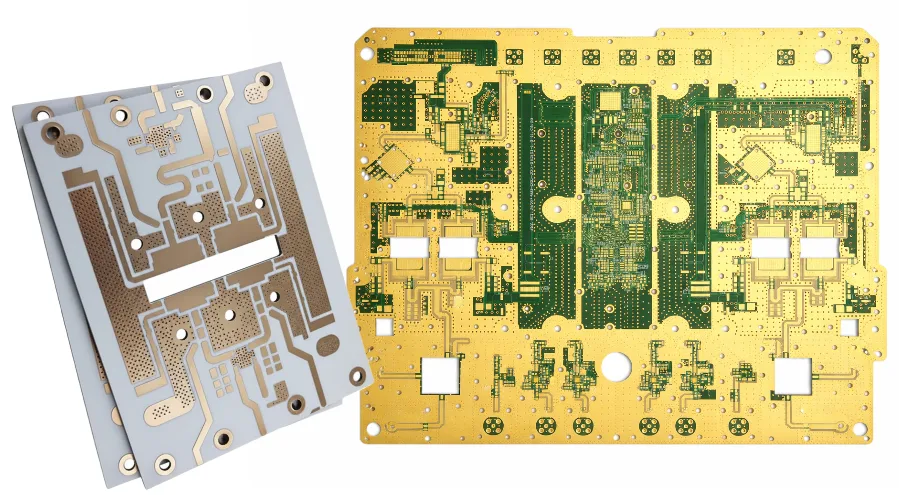
База данных материалов для печатных плат: марки и свойства ламинатов
Как получить коммерческое предложение на печатные платы? Давайте проведем анализ DFM/DFA для...
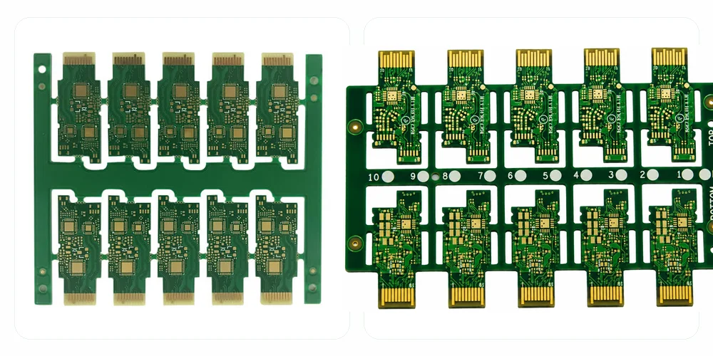
Производитель печатных плат для оптических трансиверов, специализирующийся на разработке модульных плат с возможностью индивидуальной настройки.
Компания Highleap Electronics производит и собирает продукцию по индивидуальному заказу...
Производитель печатных плат оптических модулей для программ 400G, 800G и 1.6T.
Компания Highleap Electronics производит печатные платы для оптических модулей...
Производитель печатных плат для оптической связи и волоконно-оптического сетевого оборудования.
Компания Highleap Electronics производит и собирает оптические устройства...
Как получить расценки на печатные платы
Давайте проведем для вас анализ DFM/DFA и вернемся к вам с отчетом. Вы можете безопасно загрузить свои файлы через наш веб-сайт. Для того, чтобы дать вам предложение, нам нужна следующая информация:
-
- Gerber, ODB++ или .pcb, спец.
- Список спецификаций, если вам требуется сборка
- Количество
- Время поворота
Помимо производства печатных плат, мы предлагаем широкий спектр электронных услуг, включая проектирование печатных плат, печатные платы и готовые решения. Если вам нужна помощь с прототипированием, проверкой дизайна, поиском компонентов или массовым производством, мы оказываем комплексную поддержку, чтобы гарантировать успех вашего проекта.
Для услуг PCBA, пожалуйста, предоставьте ваш BOM (спецификация материалов) и любые конкретные инструкции по сборке. Мы также предлагаем анализ DFM/DFA для оптимизации ваших проектов для технологичности и сборки, обеспечивая плавный процесс производства.