
PCB IT-958G для високошвидкісних серверів та об'єднувальних плат
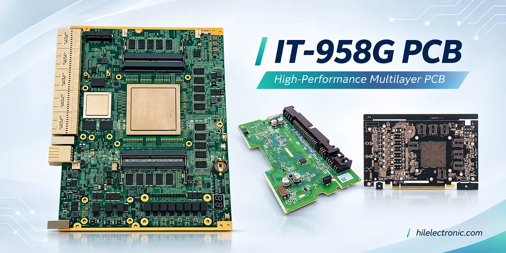
IT-958G multilayer PCB examples for server and high-speed interconnect applications.
For a server backplane or high-speed networking board, choosing a low-loss laminate is only the start: insertion loss also depends on copper profile, trace geometry, vias, connectors and channel length. IT-958G is an ITEQ low-loss material option used in server, storage and telecom PCB designs. Highleap can take a released IT-958G design through PCB fabrication and PCBA, with stack-up, impedance coupons, connector interfaces and channel acceptance criteria reviewed as one manufacturing package.
ITEQ lists IT-958G with 10 GHz Dk of 3.70 and Df of 0.0070 for a 50%-resin specimen, and Tg of 175°C by DSC. Those values support material selection but do not by themselves guarantee insertion loss for a finished channel: trace profile, copper treatment, vias and connectors can dominate parts of the loss budget.
IT-958G Material Properties for Server and Backplane PCBs
The current ITEQ IT-958G datasheet lists Dk of 3.70 та Df 0.0070 при 10 ГГц для 50% resin-content test specimen. It also reports a Tg of 175°C by DSC and 2.5% Z-axis expansion from 50°C to 260°C. The figures make sense as one possible low-loss engineering option; they do not by themselves set the maximum lane length or data rate of a finished backplane.
| IT-958G property | Типове значення, опубліковане постачальником | Impact on PCB design or fabrication |
|---|---|---|
| Dk at 1 / 2 / 5 / 10 GHz, 50% resin | 3.85 / 3.80 / 3.74 / 3.70 | Frequency and specimen conditions belong in the field-solver model |
| Df at 1 / 2 / 5 / 10 GHz, 50% resin | 0.0054 / 0.0057 / 0.0062 / 0.0070 | Loss tangent is frequency-dependent, not a single constant for every channel |
| Тг, ДСК | 175 °C | Helps screen thermal behavior, not a direct operating-temperature limit |
| Розширення по осі Z, 50–260°C | 2.5% | Requires normal through-hole stress and plating review in thick boards |
| Температура розкладання, втрата маси 5% | 400 °C | Thermal-stability characteristic under the specified test |
| T288 | Більше 60 хвилин | Material test, not a finished-board reflow qualification |
The laminate and prepreg product forms are identified as IT-958GTC and IT-958GBS. Because the published Dk/Df values refer to a defined specimen, dielectric test data matched to the actual resin and glass construction should be used for field-solver inputs. A different resin ratio or glass reinforcement can shift the effective dielectric constant seen by a trace, even when the resin-family name remains unchanged.
An important material distinction is that IT-958G is not the lowest-loss option in ITEQ’s portfolio. A higher-cost ultra-low-loss grade may be justified where dielectric loss dominates a long channel. Conversely, for a compact channel whose total loss is governed by connectors or transitions, changing to that grade may create unnecessary cost and sourcing complexity.
IT-958G server PCB manufacturing: choosing the right loss class
For a server or network equipment PCB, material cost is only one part of the choice. IT-958G provides published low-loss dielectric data, but the appropriate laminate depends on the routed length, the interface’s loss budget, via-transition count and connector model. A short, well-controlled channel may not justify a more expensive dielectric; a long backplane route may require a lower-loss grade even if IT-958G meets the nominal impedance target.
A low-loss PCB manufacturer should review the transmission-line layers, available core/prepreg constructions, foil profiles and finished trace geometry before accepting an insertion-loss target. These details are connected: changing dielectric spacing to tune impedance can also change routing density and conductor loss.
Low-Loss Backplane PCB Fabrication and IT-958G Channel Loss
Separate the causes before specifying a more expensive laminate
Розглянемо a гіпотетичний channel-loss budget totaling 10 dB at a relevant frequency: 4 dB from conductor loss, 3 dB from dielectric loss and 3 dB from connectors and discontinuities. A material change that hypothetically halves only the dielectric component would reduce the total to 8.5 dB, not 5 dB. These numbers are an educational example, not a measurement of IT-958G or a real Highleap board. The point is that improving a minor contributor can never rescue a channel whose dominant problems are launches or connectors.
The correct development sequence starts by comparing the modeled channel with its allocated loss budget. If the dielectric share is already acceptable, focus on foil, route length, stubs or topology. If the dielectric term dominates and the required margin is unattainable, a lower-Df material may be justified. That choice should remain traceable to the channel model and the approved construction.
High-speed board loss is not determined by Df alone. Dielectric loss depends on field distribution, frequency and transmission-line geometry; conductor loss depends on skin effect, copper surface profile and the finished conductor cross-section. The fabrication controls that preserve a low-loss transmission path must also account for via transitions, connector launches and reference-plane interruptions as the design moves from calculation to production.
A useful way to review the channel
- Partition the channel: identify package escape, routed stripline/microstrip segments, plated-via transitions, connector footprint and receiving-end launch.
- Assign a consistent loss model: use frequency-dependent laminate properties, measured or modeled copper treatment and appropriate conductor-geometry assumptions.
- Control the physical board: review finished width, dielectric thickness, plating, etch-back and registration tolerances with the fabricator.
- Define the validation structure: include impedance and, where required, insertion-loss coupons that represent the relevant routing layer and foil construction.
Na przykład,,en гіпотетичний 250 mm backplane run that changes layer twice cannot be evaluated using a quoted laminate Df and a straight microstrip estimate alone. The via barrels and antipad transitions can disturb impedance, while the connector footprint creates its own return-path discontinuity. A design may benefit more from better via transitions than from a modest laminate-loss improvement.
Where the unused portion of a plated barrel consumes meaningful channel margin, controlled-depth removal of unused via stubs can be specified with a residual-stub tolerance and a corresponding inspection method.
Команда copper-profile effects on conductor attenuation at high frequency are especially relevant as skin depth decreases. A rougher treatment can lengthen the effective current path and increase conductor loss, while smoother foil may require closer review of peel strength, lamination adhesion and process compatibility. The approved foil type therefore belongs in the material and fabrication specification.
Is IT-958G suitable for a long high-speed backplane?
There is no universal data-rate limit implied by the IT-958G product name. A backplane PCB carrying a relatively long differential pair must be evaluated using the transmitter/receiver channel requirements, operating frequency range, connectors, vias, conductor roughness and dielectric loss. The ITEQ Df at 10 GHz is a material-test input—not the measured dB loss of the assembled backplane.
The engineering release should distinguish a controlled-impedance target from an insertion-loss mask. Impedance can be in tolerance while conductor roughness, via stubs or connector transitions consume too much signal margin. Where the specification requires it, test coupons should represent the actual signal layer and the relevant channel structure.
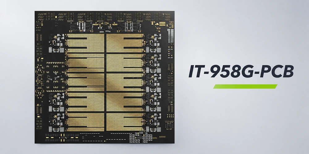
Fine-pad and routing features relevant to IT-958G fabrication and controlled-impedance review.
Controlled-Impedance Stack-Up Design With IT-958G
Fabrication compensation must match the electrical model
Artwork is commonly compensated for etching and plating because the final conductor cross-section is not an ideal rectangle. For example, narrowing at the trace top can alter both impedance and conductor loss relative to a nominal CAD rectangle, particularly on fine lines. A stack-up solver that assumes the CAD width rather than finished geometry can produce a false sense of precision. The agreed finished width, copper weight and process variation need to drive both the simulation and coupon acceptance.
If a differential pair travels near copper-plane apertures or mounting-hardware cutouts, the return current can take a longer path. The resulting mode conversion or impedance discontinuity is a routing and reference-plane defect, not proof of poor laminate quality. That is why fabrication review and signal-integrity review must share the same artwork revision.
A usable high-speed construction should identify every signal layer’s reference planes, pressed dielectric thickness and foil type. The reference-plane assignments and pressed dielectric thickness by signal layer must support both electrical objectives and a manufacturable press schedule. If a trace changes layers, the reference-plane transition and return-current path are part of the design, not optional details left to routing convention.
Electrical features that must be linked to the physical drawing
| Особливість дизайну | Potential failure if uncontrolled | Manufacturing or test response |
|---|---|---|
| Товщина пресованого діелектрика | Impedance shift even if trace artwork is unchanged | Stack-up approval, cross-section and thickness control |
| Finished trace width and edge profile | Impedance and loss differ from nominal CAD width | Etch-compensation review and coupon measurement |
| Copper foil treatment | Unexpected conductor loss or peel-strength compromise | Record approved foil profile and lamination construction |
| Reference-plane voids and split crossings | Return-path detour, mode conversion and EMI risk | Layout review and route-specific simulation |
| Via stubs / antipads | Reflection and frequency-dependent channel notches | Via model, drill data and appropriate backdrill plan if specified |
For each controlled net, the target, tolerance and coupon geometry must be defined. A nominal 100-ohm differential pair is not a complete manufacturing requirement when pressed dielectric thickness, foil type and finished trace dimensions are unspecified.
Resin and glass distribution also affect repeatability. Local glass/resin variation that can create differential-pair skew becomes more relevant as route length and timing margins tighten. Mitigation may include route-angle choices, reinforcement selection or a construction-specific glass specification.
ВИГОТОВЛЕННЯ ТА ЗБОРКА ДРУКОВАНИХ ПЛАТИ
Evaluating an IT-958G server or backplane PCB?
Highleap can discuss the board application, high-speed channel requirements and the related fabrication and PCBA scope.
Перший запит простий. No full stack-up or coupon package is needed to start. A brief description of the board and estimated quantity is enough; channel rate or impedance targets are helpful if known, and detailed test information can follow.
Server PCB Manufacturing: Lamination, Etching and Impedance Test
IT-958G’s published thermal properties do not remove the need for ordinary multilayer process control. Inner-layer treatment, resin cure, copper balance, press temperature and pressure, drilling and plating all affect the final geometry. For a board with connector-dense backplane routing and via-transition constraints, the fabricator must also control registration around large connector arrays and long plated holes.
A production-oriented control plan should keep four records connected: the material purchase description, the approved construction drawing, the coupon design and the actual board inspection report. If any one changes, the electrical model may need revision. For instance, switching the foil or replacing a low-resin prepreg with a higher-resin construction can change both trace loss and finished impedance.
The finished-board inspection plan can include cross-sections, dielectric-thickness measurements, plating verification and continuity/isolation testing. Impedance coupons verify manufactured impedance under the agreed method; they do not prove that a complete serial channel meets its eye-mask or bit-error limits. TDR verification of finished transmission-line geometry should therefore be reported separately from channel-level insertion-loss evidence.
The distinction between a modeled impedance target and an end-to-end channel measurement is a common source of unnecessary disputes. A coupon can pass while a connector launch fails; a coupon can also fail because the dielectric thickness changed, even if the bare board passes an electrical continuity test. The test plan should match the failure mechanism the customer wants to control.
Controlled-impedance PCB test versus insertion-loss verification
A TDR measurement primarily evaluates time-domain impedance discontinuities. A frequency-domain insertion-loss measurement evaluates attenuation over the specified band. Neither test can be substituted automatically for the other. For a high-speed server PCB, acceptance criteria should specify the relevant coupon geometry, measurement method, reference planes, calibration or de-embedding approach and pass/fail limits.
This matters when comparing quotes from backplane PCB manufacturers: a supplier offering only continuity and nominal impedance testing may not be quoting the same validation scope as a supplier asked for S-parameter evidence. The customer’s test specification should make the distinction explicit.
IT-958G PCB Assembly, Connector Interfaces and Release Testing
A board can pass impedance and still fail the system eye
Impedance tests characterize a specific coupon and measurement condition. A system link includes active drivers/receivers, packages, connectors and discontinuities that the coupon may not represent. If the customer requires a channel-compliance target, appropriate S-parameter measurement or system-level signal testing should be planned separately; a universal bit-error guarantee cannot be inferred from a material grade.
Press-fit connectors deserve special handling. The exact finished hole diameter, plating thickness, hole-wall quality, insertion force and board support affect connector performance. A shift in finished hole size can cause assembly damage while an electrical trace coupon remains perfect. This is a second reason to keep assembly and bare-board acceptance requirements in the same release package.
Server and storage products often combine press-fit connectors, high-pin-count packages and dense power distribution. The high-speed PCB manufacturing and assembly plans should address connector-hole geometry, plating, board flatness and solder-mask definition together. A press-fit connector can place concentrated mechanical loads near plated holes and adjacent traces; its allowed hole tolerances are not determined by the laminate Dk.
If the project includes populated boards, PCB assembly must follow the released thermal profile and board construction. BGA and QFN inspection, paste deposition and rework limits remain component- and process-specific. An IT-958G board should not be described as qualified for all soldering profiles solely because its Tg and Td meet published laminate values.
For hidden joints beneath these packages, radiographic inspection of BGA and QFN solder connections can supplement optical inspection where package geometry and the agreed quality plan warrant it.
For a detailed manufacturing review, the engineering package will ultimately define the approved stack-up and material form, drill data, controlled-impedance targets, signal-coupon requirements, copper treatment and acceptance criteria. If PCBA is included, the component list, placement information, connector details and inspection scope are also confirmed before release. An initial inquiry can start with the board application and approximate quantity; the full file set can follow when the design is ready.
Highleap Electronics can assess the requested IT-958G bare-board fabrication, agreed inspection and PCB assembly scope against those project files. Where a higher-speed or longer channel challenges the loss budget, the material comparison should be performed against measured or simulated channel needs rather than assuming that a lower-Df name automatically guarantees performance.

Про автора
Sabrina
Спеціаліст з інженерії друкованих плат у Highleap Electronics
Сабріна має понад 18 років досвіду роботи в галузі друкованих плат, а також великий досвід у CAM-інженерії та перевірці файлів друкованих плат. Вона підтримує проекти друкованих плат від прототипу до серійного виробництва, зосереджуючись на технологічності та надійності процесу.
Її робота допомагає інженерним командам знизити виробничі ризики та досягти стабільних, високоякісних результатів у виробництві друкованих плат.

Рекомендовані повідомлення
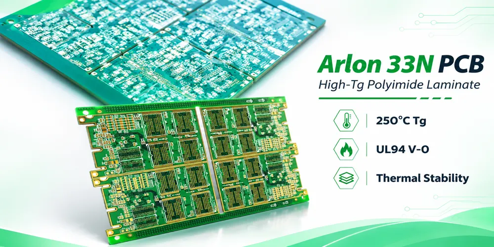
Виробництво високоякісних друкованих плат Arlon 33N
Ілюстрація виробництва друкованої плати. Підтвердьте зазначене...
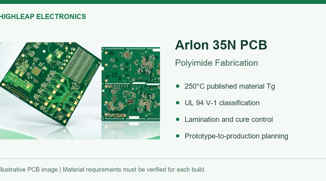
Виробництво друкованих плат Arlon 35N та ламінування поліімідом
Ілюстрація виробництва друкованої плати. Підтвердьте зазначене...
Виготовлення друкованих плат Arlon 45NK з низьким CTE в Китаї
Ілюстрація виробництва друкованої плати. Підтвердьте зазначене...

Послуги з виробництва друкованих плат Arlon 85HP у Китаї
Ілюстрація виробництва друкованої плати. Підтвердьте зазначене...
Як отримати цінову пропозицію на друковані плати
Давайте проведемо для вас аналіз DFM/DFA та надамо вам звіт. Ви можете безпечно завантажити свої файли через наш вебсайт. Нам потрібна наступна інформація, щоб надати вам цінову пропозицію:
-
- Gerber, ODB++ або .pcb, спец.
- Список специфікації, якщо вам потрібна збірка
- Кількість
- Час повороту
Окрім виробництва друкованих плат, ми пропонуємо повний спектр електронних послуг, включаючи проектування друкованих плат, виготовлення друкованих плат (PCBA) та комплексні рішення. Незалежно від того, чи потрібна вам допомога з прототипуванням, перевіркою проекту, пошуком компонентів чи масовим виробництвом, ми надаємо комплексну підтримку, щоб забезпечити успіх вашого проекту.
Для послуг з виготовлення друкованих плат (PCBA), будь ласка, надайте свою специфікацію матеріалів (BOM) та будь-які конкретні інструкції зі складання. Ми також пропонуємо аналіз DFM/DFA для оптимізації ваших конструкцій для технологічності та складання, забезпечуючи безперебійний виробничий процес.