
Производство печатных плат для портативных эндоскопических камер для OEM-производителей.
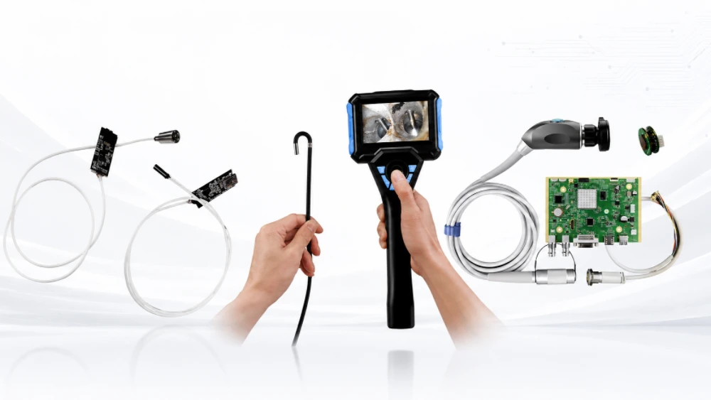
Печатная плата портативной эндоскопической камеры может относиться к электронике для промышленного контроля или к электронике камер, предназначенных для регулируемых медицинских изделий. Базовое оборудование может включать миниатюрные CMOS-сенсоры, светодиодную подсветку, узкие кабели зонда и платы обработки изображений, однако производственная документация, валидация, отслеживаемость и нормативные обязательства могут существенно различаться. Эти категории применения не следует объединять в одну общую заявку.
С точки зрения проектирования печатных плат и сборок, наиболее сложной характеристикой обычно является головка камеры. Доступный диаметр может вынуждать использовать очень маленькие компоненты, тонкие жесткие платы, гибкие печатные платы, переходники между жесткими и гибкими платами или структуры HDI. Затем кабель зонда должен передавать данные изображения и питание по длинному узкому пути, в то время как основная электроника обеспечивает обработку, отображение, USB- или беспроводное соединение и управление батареей.
Компания Highleap Electronics может оказывать поддержку заказчику в изготовлении и сборке жестких, гибких и жестко-гибких печатных плат, если эти технологии присутствуют в утвержденном проекте, а также в поиске компонентов, программировании и функциональном тестировании по запросу заказчика. Данная статья посвящена технологичности производства и не претендует на получение медицинских сертификатов или одобрения регулирующих органов для готовых устройств без соответствующего разрешения.
Требования к печатным платам для промышленных и медицинских эндоскопов должны быть разделены.
Промышленные эндоскопы широко используются в машиностроении, автомобильной и аэрокосмической промышленности, при прокладке труб и в труднодоступных местах. При проектировании к приоритетам могут относиться диаметр зонда, прочность кабеля, водонепроницаемость, освещение и качество изображения. Электроника медицинских эндоскопов может использовать аналогичные миниатюрные методы визуализации, но может предъявлять дополнительные требования к управлению рисками, контролю конструкции, отслеживаемости, материалам, совместимости с системами очистки или стерилизации, а также к регулируемым системам качества в зависимости от устройства и рынка.
| Район | Продукция для промышленного контроля | Программа медицинских изделий |
|---|---|---|
| Миниатюризация печатных плат | Определяется геометрией зонда и требованиями к изображению. | Определяется геометрией зонда, а также специфическими для устройства ограничениями безопасности/валидации. |
| Прослеживаемость | Коммерческий/OEM-определенный | Может потребоваться более строгая отслеживаемость устройства/партии/технологического процесса. |
| Материалы | Экологические потребности и требования к надежности | Может включать дополнительные контролируемые аспекты материалов/биосовместимости на уровне продукта. |
| Очистка/стерилизация | Специализированная прочность для конкретных областей применения | Может взаимодействовать с требованиями к стерилизации и подтвержденной обработке. |
| Документация по качеству | договорные требования OEM | Применимые регулируемые требования к системе качества должны быть определены производителем медицинского изделия. |
| Калибровка/проверка | Качество изображения и контроля | Проверка производительности на уровне устройства и соответствие нормативным требованиям, выходящие за рамки обычных испытаний печатных плат. |
Поэтому поставщик печатных плат должен запрашивать спецификацию конечного потребителя, а не делать вывод о соответствии из слова «эндоскоп». Если заказчик медицинских изделий требует определенных сертификатов, подтверждения технологических процессов или документации, эти требования должны быть подтверждены непосредственно перед предоставлением коммерческого предложения. Их ни в коем случае нельзя придумывать в рекламных материалах.
Для обеих категорий техническая отправная точка одинакова: определить головку камеры, кабель и основную плату обработки как единую систему. Различия проявляются в документации, управлении технологическими процессами и квалификации готовой продукции.
Типичная архитектура электроники эндоскопической камеры
Некоторые датчики камер интегрируют большой объем обработки изображений и передают последовательный поток, в то время как другим требуется дополнительная поддержка со стороны хоста. Выбранный датчик определяет параметры питания, тактовой частоты, пропускную способность интерфейса, количество проводников и количество локальных компонентов. Команда разработчиков должна получить точную техническую документацию на датчик и утвержденные ограничения эталонного проекта, а не только разрешение камеры.
Архитектура может также включать отдельную плату подсветки, плату дистального датчика и плату проксимального интерфейса. В чрезвычайно узких зондах компоненты могут быть распределены вдоль гибкой цепи, а не сконцентрированы на одном жестком конце. Это механико-электрическое разделение необходимо утвердить до выпуска окончательных чертежей для изготовления печатной платы, поскольку оно напрямую определяет зоны изгиба, ребра жесткости и несущие элементы сборки.
Полезный запрос предложений (RFQ) определяет, какие именно узлы Highleap должна изготовить. Изготовление гибких плат, поверхностный монтаж головки камеры, крепление кабеля, сборка материнской платы и окончательная оптико-механическая сборка — это отдельные операции. Объединение их в рамках концепции «эндоскоп под ключ» без чертежей делает неясными затраты и распределение ответственности.
Миниатюризация печатной платы эндоскопической камеры
Миниатюризация — это не просто уменьшение габаритов платы. По мере уменьшения диаметра зонда начинают взаимодействовать корпус компонента, диаметр переходных отверстий, количество слоев, высота разъема и геометрия паяльной маски. Разводка, которая помещается в САПР, может не оставлять достаточного запаса для производственной трассировки, сборки или разделения на панели.
Размер упаковки компонента
Компактные пассивные компоненты и сенсорные корпуса с малым шагом выводов позволяют уменьшить габариты, но при этом увеличивают требования к трафаретной съемке, размещению и контролю качества. Сверхмалые корпуса следует использовать там, где они решают реальную проблему ограничения диаметра или высоты, а не в качестве стандартного признака передовой конструкции. Более крупные варианты корпусов могут повысить выход годных изделий и упростить поиск поставщиков, если позволяет механическое пространство.
HDI и микропереходы
Использование HDI может стать необходимым, когда трассировка BGA/WLCSP с малым шагом выводов или плотная трассировка выводов датчиков невозможна с помощью сквозных переходных отверстий. Микропереходные отверстия и переходные отверстия в контактной площадке уменьшают препятствия при трассировке, но они добавляют этапы изготовления и требуют совместимой структуры контактных площадок для сборки. В утвержденной схеме расположения компонентов должны быть указаны глубина глухих переходных отверстий, требования к заполнению/закрытию и любые многослойные или смещенные структуры. Производителю печатных плат не следует импровизировать с этими параметрами на этапе составления сметы.
Толщина доски
Тонкие жесткие платы или гибкие печатные платы могут помочь разместить узкий зонд, но механическая жесткость уменьшается с уменьшением толщины. Во время сборки печатную плату может потребоваться поддерживать корпусом линзы или усилителем. Плата, пригодная для электрических испытаний, но деформирующаяся при размещении датчика, может создавать проблемы с оптической юстировкой.
устранение разъема
Использование технологии Rigid-flex позволяет обойтись без миниатюрного разъема между удаленной камерой и кабелем, что экономит высоту и снижает вероятность сбоев контакта. Компромисс заключается в более сложной конструкции печатной платы и меньшей модульности замены. Инженерам следует сравнивать общий объем сборки и надежность, а не только стоимость самой печатной платы.
Гибкая и жестко-гибкая конструкция зонда камеры
Гибкие печатные платы (Flex PCB) привлекательны для эндоскопов, поскольку позволяют прокладывать кабели через узкие изогнутые пространства, передавая сигналы датчиков, питание светодиодов и управляющие сигналы. Жестко-гибкие платы (Rigid-flex) обеспечивают стабильные участки для компонентов на дистальном или проксимальном концах. Ни одна из этих технологий не является обязательной; выбор зависит от механики зонда и объема производства.
| Гибкий элемент дизайна | Почему это важно для производства |
|---|---|
| Статический и динамический изгиб | Определяет способ прокладки медных проводников, радиус изгиба и ожидаемые показатели усталости материала. |
| Зазоры, покрытые защитным покрытием | Контролирует контактные площадки для пайки и геометрию сборки с малым шагом выводов. |
| Ребра жесткости | Поддержка разъемов, датчиков и паяных соединений во время сборки/использования |
| Переход от жесткого к гибкому состоянию | Требуется контролируемое завершение слоя и снятие механических напряжений. |
| Панельизация/перевозчик | Обеспечивает достаточную плоскость тонкого гибкого материала для печати и позиционирования. |
| Стопка клея/материала | Влияет на толщину, гибкость, тепловые характеристики и совместимость с технологическими процессами. |
Компоненты не следует размещать в зоне изгиба, если в конструкции явно не учтены деформации. Проводники должны плавно переходить через зоны изгиба, и следует по возможности избегать резких сужений на границах жесткого и гибкого участков. Изготовитель может предложить каплевидную форму, изменения в покрытии или опоре панели, но любое изменение в жестко закрепленном зонде следует довести до сведения инженерного отдела, поскольку оно может повлиять на механические характеристики.
Для сборки гибкий кабель может быть временно приклеен или закреплен в несущей панели. Конструкция паллеты для пайки оплавлением становится особенно важной, когда плата имеет тяжелый датчик изображения на одном конце и тонкий хвостовик на другом. После сборки инструкции по обращению должны предотвращать использование операторами хвостовика гибкого кабеля в качестве рычага при перемещении или осмотре головки камеры.
Поддержание целостности сигнала при использовании длинного эндоскопического кабеля.
Передача высокоскоростных изображений по узкому кабелю зонда сопряжена с теми же фундаментальными проблемами, что и любой другой путь передачи: затухание, разрыв импеданса, перекрестные помехи и прерывание обратного пути. Сложность заключается в том, что механический кабель может предоставлять гораздо меньше свободы, чем широкая печатная плата. Поэтому выбор интерфейса необходимо проверять на предполагаемой длине кабеля, предназначенного для серийного производства, а не только на оценочной плате.
Переходы от печатной платы к кабелю могут доминировать в канале связи.
Дистальный вывод сигнала с платы, гибкий проводник, паяное соединение или разъем, кабель и проксимальный приемник следует рассматривать как один канал. Заземляющие контакты должны передаваться через переходы так, как это предусмотрено интерфейсом. Даже в дифференциальной паре, хорошо проложенной на обеих печатных платах, может наблюдаться серьезный разрыв, если распиновка разъема отделяет пару от ее обратных путей.
Электроэнергия и передача данных проходят по одному и тому же узкому механическому пути.
Ток датчика изображения и светодиода вызывает падение напряжения в кабеле. Это может изменить локальные логические пороги или внести помехи в заземление датчика. В конструкциях для управления этим процессом может использоваться локальная стабилизация или несколько заземляющих/силовых проводников. На чертеже кабеля, предназначенного для производства, должно быть указано распределение проводников, и нельзя допускать замену, казалось бы, эквивалентного кабеля только по внешнему диаметру.
экранирование
Экранирование может уменьшить внешние помехи и сдержать излучение от камеры, но оконечная нагрузка является частью конструкции. Экранирование, подключенное в неправильной точке, может создать нежелательные пути протекания тока. На сборочном чертеже должно быть указано, к чему подключается экран кабеля: к заземлению печатной платы, к шасси или к другому источнику сигнала, а также как осуществляется механическое оконечное соединение.
Функциональное тестирование должно включать проверку на максимально допустимую длину кабеля для производства или с использованием другого проверенного симулятора канала. Короткий кабель в приспособлении может скрывать проблемы с запасом прочности, которые проявляются только после окончательной сборки зонда.
Проблемы сборки печатной платы головки камеры
Дистальная часть головки камеры может представлять собой одну из наиболее рискованных печатных плат в изделии, поскольку она сочетает в себе сложную геометрию, оптические поверхности и ограниченный доступ для ремонта. Небольшой дефект пайки, который легко устранить на большой материнской плате, может привести к браку после того, как камера будет припаяна к корпусу зонда.
Миниатюрные SMD-корпуса и корпуса с малым шагом выводов.
Для нанесения пасты методом трафаретной печати необходима достаточная поддержка под тонкой платой или гибким печатным платом. Конструкция трафаретного отверстия должна обеспечивать баланс между крошечными пассивными компонентами и более крупными контактными площадками для датчиков или светодиодов. Ориентиры для размещения должны оставаться видимыми после панельной сборки. Если датчик представляет собой корпус WLCSP или другой корпус со скрытыми соединениями, рентгеновское исследование может быть полезно в зависимости от структуры контактных площадок и рисков.
Выравнивание датчика
Размещение датчика в SMT-системе определяет его положение относительно реперных точек печатной платы, но окончательная оптическая ось также зависит от допуска по контуру платы, держателя линзы, базовых точек корпуса и клея. На чертеже следует указать, какие края или отверстия печатной платы являются механическими базовыми точками, чтобы производитель понимал, что это не просто границы трассировки.
Размещение светодиодов
Расположение светодиода вокруг датчика влияет на симметрию освещения. Если в конструкции используются несколько длин волн или разные типы светодиодов, спецификация материалов и файл размещения должны точно отображать каждую деталь. Неправильно расположенный светодиод может загореться и пройти базовый электрический тест, но не соответствовать оптическим требованиям.
Оптическая чистота
Для удаления пыли и остатков вблизи датчика необходимы специальные меры предосторожности. Инструкция по работе с головкой камеры может предусматривать снятие защитной пленки на определенном этапе, использование чистых контейнеров для хранения или осмотр под увеличением. Эти меры следует отличать от общей очистки платы, поскольку на химически чистой поверхности все еще могут содержаться оптически видимые частицы.
Основная печатная плата для обработки изображений, интеграция питания и беспроводной связи.
Основная печатная плата обычно имеет более традиционные производственные сложности: процессор или микроконтроллер, память, разъем дисплея, USB, хранилище данных, Wi-Fi/BLE и зарядка батареи. В зависимости от пропускной способности видеосигнала и типа процессора, плата может потребовать многослойной трассировки с контролируемым импедансом, вывода сигнала через BGA-корпус или HDI-корпуса.
Основная печатная плата также должна изолировать интенсивную цифровую и силовую активность от входящего интерфейса камеры. Размещение импульсных стабилизаторов, переходные процессы USB и беспроводные радиочастотные помехи могут снизить запас прочности канала связи или создать видимые артефакты. Поэтому надежная структура заземления/опорного напряжения и контролируемый вывод сигнала из разъема полезны, даже несмотря на то, что чувствительный датчик изображения физически удален на конце зонда.
Нагрев аккумулятора и процесса зарядки
Портативные дисплеи могут нагреваться во время зарядки или непрерывной обработки изображений. Этот нагрев может не оказывать прямого воздействия на удаленный датчик при прокладке длинного кабеля, но может повлиять на производительность процессора и надежность корпуса. Тепловые переходные отверстия, распределение меди и механическая проводимость должны соответствовать заявленной конструкции системы охлаждения.
Варианты прошивки и датчиков камеры
Модули камер с одинаковым разрешением могут использовать разные наборы регистров или калибровочные данные. При производстве необходимо связать точную спецификацию датчика с соответствующим образом прошивки. Если конструкция поддерживает несколько типов датчиков, заводу потребуется матрица артикулов для комбинаций датчик/кабель/материнская плата, а не один универсальный программный файл.
Тестирование, оптическая валидация и границы производства для медицинского применения.
Тестирование печатных плат позволяет проверить электронику перед окончательной проверкой устройства. Типичные проверки включают загрузку процессора, связь с датчиками, видеопоток в реальном времени, работу светодиодов, целостность кабелей, функции дисплея/USB/беспроводной связи и зарядку. Тестирование с помощью мишени может выявить проблемы с фокусировкой или грубые дефекты изображения, если приспособление и правила прохождения/непрохождения определены производителем оборудования.
Тестирование изображений не заменяет проверку готового устройства.
Фокусировка, разрешение, освещение, искажения и цветопередача зависят от линзы, корпуса и собранного зонда. Для медицинских изделий может потребоваться дополнительная проверка безопасности и производительности в соответствии с применимой классификацией устройства и рынком. Завод по производству печатных плат не должен представлять проверку изображения на экране в качестве доказательства соответствия медицинским изделиям.
Стерилизация и совместимость материалов являются входными параметрами проектирования на уровне продукта.
Если медицинский эндоскоп или принадлежность предназначены для стерилизации или многократной очистки, материалы печатных плат, клеи, герметики, оболочки кабелей и оптические уплотнения должны выдерживать определенный технологический процесс. Эти требования должны быть прописаны в утвержденной конструкции производителя медицинского оборудования. Компания Highleap должна производить продукцию в соответствии с предоставленными спецификациями, а не заявлять об универсальном рецепте «печатных плат медицинского класса».
Прослеживаемость
В рамках программ может потребоваться прослеживаемость на уровне партии или на уровне единицы продукции для данных печатных плат, датчиков, встроенного программного обеспечения или калибровки. Требуемая глубина прослеживаемости должна быть указана в запросе предложений, поскольку она влияет на маркировку, обработку баз данных и производственную документацию. Компания Highleap может предложить и реализовать только ту прослеживаемость, которая была технически определена для проекта.
От прототипа до серийного производства: что отправлять поставщику печатных плат
При создании прототипов необходимо проверить не только электрическую функциональность. Команда должна подтвердить диаметр зонда, поведение при изгибе, потери в кабеле, температуру светодиода, оптическую юстировку, артефакты изображения, удобство сборки и доступ для тестирования. Если головку камеры можно собрать только вручную под микроскопом, это может быть приемлемо для десяти прототипов, но дорого и ненадежно для тысяч единиц.
В пилотном производстве следует использовать гибкую сборку, кабель, датчик, интерфейс линзы и приспособление, предназначенные для серийного производства. На этом этапе необходимо зафиксировать панельную структуру, несущие элементы, профиль оплавления, очистку/обработку, программирование и тестирование изображений. В программах для медицинских изделий также следует убедиться, что необходимые технологические записи и мероприятия по валидации определены до начала серийного производства.
Пакет запроса коммерческого предложения
- Файлы Gerber/ODB++, а также чертежи для изготовления жестких, гибких или жестко-гибких печатных плат и схемы сборки.
- Требования к разъемам HDI/microvia/via-in-pad там, где они используются в головке камеры.
- Спецификация компонентов, утвержденные альтернативные варианты и точные номера деталей датчика изображения/светодиода.
- Чертежи для операций захвата и перемещения, а также сборки с использованием оптических/механических базовых точек.
- Чертежи кабелей/гибких проводов, распиновка, длина и требования к экранированию/концевой части.
- Инструкции по хранению, пайке оплавлением, очистке и обращению с датчиком.
- Программные файлы, матрица артикулов датчиков/зондов и требования к сериализации.
- Спецификация функционального/визуального тестирования и любые этапы калибровки на уровне продукта указываются отдельно.
- Любые требования к качеству, отслеживаемости или валидации процессов медицинских изделий, прямо установленные производителем оригинального оборудования (OEM).
- Объемы производства прототипов, опытных образцов и прогнозируемые объемы производства.
Комплексное решение позволяет Highleap Electronics точно рассчитать стоимость работ по изготовлению печатных плат/сборок, не обещая при этом необоснованных обещаний относительно проектирования готовых устройств или услуг по соблюдению нормативных требований. Для промышленных программ это может означать сборку миниатюрной камеры и основного контроллера. Для регулируемых медицинских программ дополнительные требования к качеству/технологическим процессам могут быть рассмотрены только после их предоставления заказчиком.
Целью производства является сохранение исходной геометрии головки камеры, канала для гибкого кабеля, оптической чистоты, спецификации материалов и результатов производственного тестирования по мере масштабирования проекта. Это практический путь от работающего миниатюрного прототипа к воспроизводимой сборке печатной платы эндоскопической камеры.
Часто задаваемые вопросы
В чём разница между платой для бороскопа и платой для эндоскопа?
Электронные архитектуры могут быть схожими, но термин «эндоскоп» может включать в себя регулируемые медицинские изделия с дополнительными требованиями к качеству, валидации, отслеживаемости и соблюдению нормативных требований. Эти требования должны определяться отдельно от обычного производства печатных плат для промышленных камер.
Можно ли использовать гибкие печатные платы внутри зонда эндоскопической камеры?
Да. Гибкие печатные платы позволяют прокладывать кабели через узкие изогнутые пространства и уменьшать объем разъемов. Жестко-гибкие кабели могут обеспечивать стабильные блоки компонентов, а также интегрированные гибкие межсоединения, но ни то, ни другое не является обязательным для каждой конструкции.
В каких случаях для печатной платы эндоскопической камеры требуется HDI?
Технология HDI становится полезной в тех случаях, когда диаметр зонда, шаг корпуса или плотность трассировки не могут быть экономически достигнуты с помощью обычных сквозных отверстий. Она должна определяться фактическими ограничениями по выходу и механическими свойствами.
Почему оптическая чистота важна при сборке печатных плат?
Пыль, флюсовая пыль или другие частицы вблизи датчика или объектива могут появляться на изображении, даже если плата исправна с электрической точки зрения. Поэтому для сборки головки камеры может потребоваться специальная обработка и оптический осмотр.
Как следует проверять целостность сигнала с помощью длинного измерительного кабеля?
Проверьте весь путь кабеля, используя заданную длину и переходы, включая дистальную плату, кабель/разъем и основную печатную плату приемника. Короткий кабель для разработки может скрывать проблемы с затуханием или импедансом.
Распространяется ли автоматическая сертификация медицинских изделий Highleap на проекты по созданию эндоскопов?
Сертификация не должна считаться подтвержденной, если она не была явно подтверждена для требуемой области применения. Разработчики медицинских изделий должны предоставить для проверки соответствующие требования к качеству, валидации, отслеживаемости и регулированию.
Какую информацию должен предоставить поставщик печатных плат для эндоскопов?
Предоставьте чертежи печатных плат/гибких плат, данные о структуре слоев и HDI, спецификацию материалов, чертежи размещения/сборки, технические характеристики камер и кабелей, инструкции по обращению, файлы программирования/тестирования, необходимую прослеживаемость и ожидаемые объемы.
Производственные требования следует сверять с выпущенными проектными файлами, спецификациями производителей компонентов и применимыми требованиями к валидации или регулированию конечного продукта.

Рекомендуемые сообщения

Производство фильтрующих печатных плат TMM4
Производство печатных плат с фильтрами TMM4 контролируется...

Производство печатных плат TMM3 для радиочастотных модулей
Производство печатных плат TMM3 наиболее полезно в тех случаях, когда используется радиочастотный модуль...

Изготовление печатных плат TMM6
Изготовление TMM6 — это страница управления технологическим процессом для среднего Dk...

Изготовление печатных плат TMM10 для компактных радиочастотных схем
Содержание: Как TMM10 уменьшает размеры ВЧ-структур; TMM10 против...
Как получить расценки на печатные платы
Давайте проведём для вас анализ DFM/DFA и предоставим отчёт. Вы можете безопасно загрузить свои файлы через наш сайт. Для составления коммерческого предложения нам необходима следующая информация:
-
- Gerber, ODB++ или .pcb, спец.
- Список спецификаций, если вам требуется сборка
- Количество
- Время поворота
Для услуг PCBA, пожалуйста, предоставьте ваш BOM (спецификация материалов) и любые конкретные инструкции по сборке. Мы также предлагаем анализ DFM/DFA для оптимизации ваших проектов для технологичности и сборки, обеспечивая плавный процесс производства.