
便携式二氧化碳监测仪PCB设计与制造指南
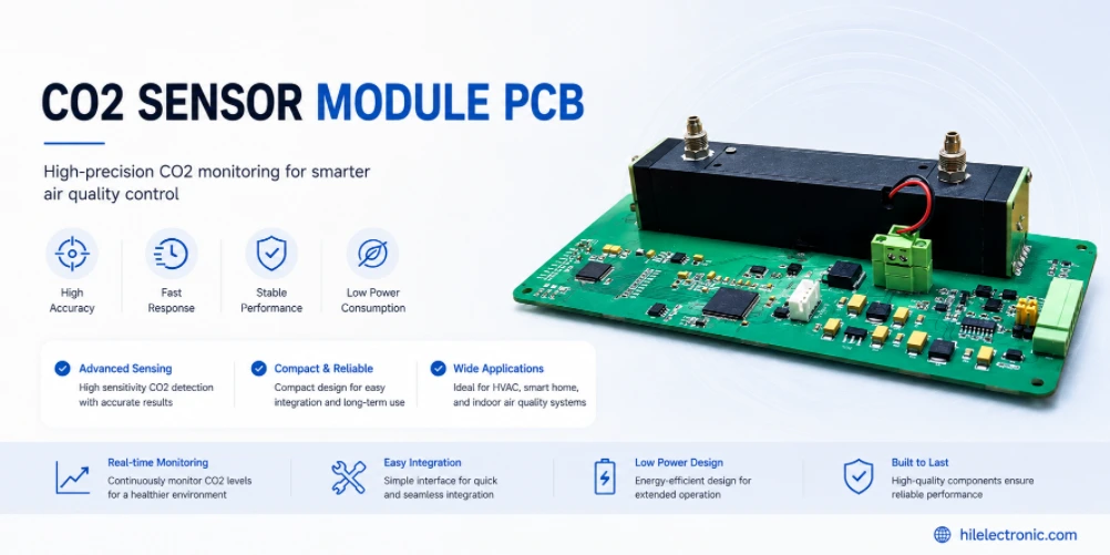
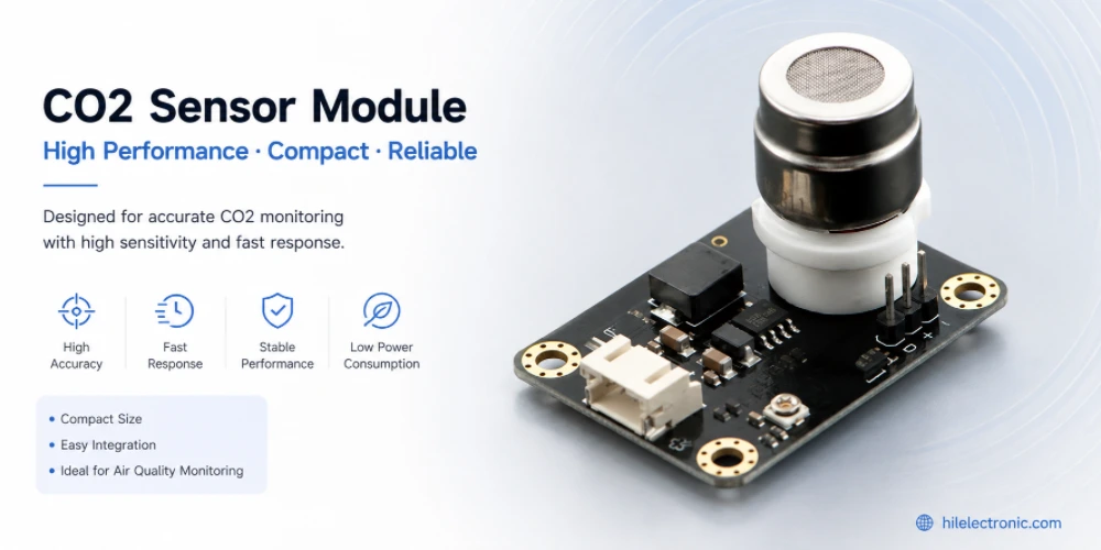
A portable CO2 monitor PCB has to support accurate gas measurement while operating inside a small battery-powered enclosure that also contains processors, displays, charging circuits and, in many products, wireless radios. Those blocks can create heat, supply transients and electromagnetic noise that influence the environment around the sensor. For engineering teams, the board is therefore not just a controller: it is part of the measurement system.
The manufacturing path should follow the released sensor architecture. A monitor built around a self-contained NDIR module with UART or I²C can be comparatively straightforward, while a smaller custom sensing platform can place more responsibility on the main PCB for power integrity, compensation, mechanical airflow and calibration handling. Highleap Electronics can manufacture customer-owned PCB and PCBA designs, source components, assemble prototypes and production lots, and execute customer-defined programming or functional tests without implying responsibility for the finished instrument design or its environmental certification.
The sections below focus on the decisions that affect PCB fabrication, PCB assembly and production repeatability: sensor integration, thermal placement, airflow, low-noise power, stack-up, component sourcing, test boundaries and RFQ documentation.
Portable CO2 Monitor Product Architecture and System Scope
Most buyers searching for a portable CO2 monitor PCB are not looking for a definition of carbon-dioxide sensing. They are usually trying to solve a hardware integration or sourcing problem: how to connect a gas sensor reliably, keep battery life acceptable, fit the board into the enclosure, and move from prototype PCBA into repeatable production. A useful engineering article therefore starts from the architecture rather than from general indoor-air-quality education.
A typical board may carry the MCU, battery charger, voltage regulators, display connector, buttons, buzzer, status LEDs, memory and optional BLE or Wi-Fi circuitry. The CO2 sensor may be soldered directly, mounted through pins, attached by a cable, or treated as a replaceable module. Temperature and relative-humidity sensing may also be present because the product uses those measurements for display, compensation or environmental context.
| 子系统 | 典型的设计问题 | PCB/PCBA impact |
|---|---|---|
| 二氧化碳传感器 | Module, SMT device or connector-mounted assembly? | Footprint, height, reflow limits, airflow clearance and sourcing |
| MCU / interfaces | UART, I²C, ADC or vendor-specific interface? | Routing, level compatibility, programming access and test points |
| Display / UI | LCD, OLED, buttons, LEDs, buzzer? | FPC/connectors, current transients and mechanical alignment |
| 电力 | Li-ion/LiPo, USB-C, replaceable cells? | Charging, protection, regulators, thermal placement and battery connector |
| 连接方式 | BLE/Wi-Fi required? | RF keep-out, antenna placement, emissions and current peaks |
| 记录 | Local flash or removable storage? | BOM, routing density and firmware/test requirements |
NDIR Sensor Integration, Airflow and Thermal Placement
NDIR sensors measure CO2 optically and many commercial modules expose digital interfaces rather than a raw low-level analog signal. That simplifies the host PCB, but it does not remove mechanical constraints. The sensor must still sample representative ambient air, and the enclosure must not trap a pocket of heated air around it. A sensor placed beside a charger IC, backlit display or switching regulator can operate in a local thermal environment that differs from the room the product is intended to measure.
Sensor mounting is a manufacturing choice as well as a design choice
Some CO2 sensors are compatible with SMT processing, while others use pin headers, through-hole leads, board-to-board connectors or cables. The component manufacturer’s storage, soldering and reflow limits should define the process. A PCBA supplier should not automatically push a large optical module through the same reflow profile used for the MCU simply because the footprint appears solderable. If the module is installed after reflow, the assembly drawing should state the insertion sequence, orientation, hardware and any manual soldering limits.
Air openings and keep-out areas need to survive DFM
The electrical design can be correct while the final monitor performs poorly because the enclosure blocks the sensor inlet or a foam gasket changes airflow. PCB DFM should preserve mechanical keep-outs around sensor openings, vents and optical cavities. Panel tabs, tooling holes, conformal coating and cleaning processes should also be reviewed so they do not contaminate or obstruct the sensing path. The same caution applies to adhesives and potting materials near the sensor.
Temperature and humidity sensors deserve their own placement review. If they are intended to represent ambient conditions, mounting them next to the battery charger, MCU or RF power amplifier can introduce self-heating bias. In compact products, engineers may use board-edge placement, cutouts, thermal isolation features or controlled duty cycles, but the correct approach depends on the enclosure and sensor vendor guidance rather than on a universal PCB rule.
Low-Noise Power, Grounding and Battery Management
Portable monitors combine a sensing subsystem with several noisy or pulsed loads. USB charging, a buzzer, display backlight, wireless transmitter and switching converter can all create current steps. The CO2 sensor itself may also draw a very different peak current than its long-term average. The power architecture should therefore be checked against peak demand, not only the average number used in a battery-life spreadsheet.
Local decoupling should follow the component manufacturers’ recommendations, with short current loops and low-impedance return paths. If the sensor needs a particularly clean rail, designers may use filtering, a dedicated regulator or an LDO after a switching converter. That choice is a trade-off: an LDO can reduce switching noise but wastes power when the voltage drop is large, while a DC-DC converter improves efficiency but introduces switching edges that must be controlled by placement and layout.
Do not split grounds by label alone
A common mistake is to create “analog ground,” “digital ground” and “sensor ground” islands without understanding where currents return. For many monitor architectures, a continuous reference plane with deliberate placement of noisy loops gives more predictable behavior than fragmented ground copper. If the sensor vendor specifies a particular grounding arrangement, that reference design should take priority. The assembler’s DFM process should also avoid adding copper pours or moving return vias in electrically sensitive zones without design approval.
Battery charging is also a thermal problem
Charging a small Li-ion or LiPo cell inside a sealed enclosure can raise the local temperature. The charger, protection FETs and power-path components should be placed with both electrical and thermal behavior in mind. When a temperature sensor is used for environmental reporting, the team should test the product while charging, after charging and during wireless activity. A board that measures accurately on a bench supply may behave differently when the real battery and enclosure are installed.
2-Layer vs 4-Layer PCB, FR-4 and Surface Finish
There is no fixed layer count for a portable CO2 monitor. A simple module-based design can often be routed on two layers if the board area is generous and the RF or display requirements are modest. A four-layer construction becomes more attractive when the product is compact, contains wireless connectivity, needs a more continuous ground reference, or has several power domains and dense connectors.
| 决策区 | 2-layer may be reasonable when… | 4-layer may be preferable when… |
|---|---|---|
| 路由密度 | Large board, few interfaces and simple module connections | Compact enclosure, dense MCU/display/RF routing |
| 接地参考 | Return paths can remain short and well controlled | Continuous plane materially improves return paths and EMI behavior |
| 无线耳机 | Pre-certified module with forgiving placement | Integrated RF or antenna environment is crowded |
| 电力 | Few rails and modest current | Multiple rails, charging and pulsed loads need cleaner distribution |
| Cost | Bare-board simplicity matters and design remains robust | Assembly yield and electrical margin justify extra layers |
Standard FR-4 is suitable for many portable monitors. Material selection should be driven by temperature, mechanical thickness, dielectric requirements and product environment. Likewise, copper weight should be selected from actual current and thermal needs rather than from the belief that a portable sensor product needs unusually heavy copper.
Portable CO2 Monitor PCBA: SMT, Connectors and Component Sourcing
The assembly can mix fine-pitch digital components with mechanically large modules. Typical SMT parts include an MCU, charger, regulators, memory, humidity sensor and passives. USB-C, display FPC connectors, battery connectors and board-to-board headers introduce different solder-joint and mechanical risks. The CO2 module itself may require a secondary process after the main SMT reflow.
Stencil and reflow planning should reflect the mixed component set
A thermal-pad QFN may need carefully controlled paste volume, while a USB-C connector can require robust anchor joints and good paste transfer across a very different pad geometry. A large optical sensor can shadow smaller parts or create thermal mass. Panelization and component orientation can therefore influence assembly yield. These are classic DFM/DFA questions that are better resolved before the first prototype is released than after a low-volume batch shows intermittent connectors or tombstoned passives.
BOM control matters most around the sensor, power and wireless sections
A procurement substitute that is harmless on a status LED may be unacceptable in the sensor supply, regulator feedback network, crystal, antenna match or precision compensation path. The BOM should contain manufacturer part numbers and clear alternate rules. For long-lived industrial or building-monitoring products, engineers should also identify parts with allocation or lifecycle risk before committing to a mechanical design that accepts only one obscure package.
When a wireless module is used, the exact module revision and antenna configuration should be locked to the product build. When the RF function is implemented directly on the main PCB, the matching network and antenna region require stronger change control. In both cases, the assembler should treat do-not-substitute items as controlled parts rather than cost-optimization candidates.
Programming, Functional Test and CO2 Calibration Are Different Tasks
A high-conversion RFQ needs a clear test boundary. A PCBA factory can program firmware, verify supply rails, communicate with the CO2 sensor, exercise the display, check buttons and buzzer, confirm charging, and run customer-defined current or communications tests. Those checks establish that the assembly is built correctly. They do not automatically establish the accuracy of the finished CO2 instrument.
What a production functional test can reasonably cover
- Power-on current and major rail voltages within customer-defined limits.
- MCU programming, firmware version and serial-number handling.
- Communication with the CO2, temperature and humidity sensors.
- Display, LED, buzzer, button and storage functions.
- USB charging and battery-detection behavior where the fixture supports it.
- BLE or Wi-Fi communication checks using a customer-approved procedure.
Calibration needs a defined reference and process owner
If the product requires zero-point, span, background or multi-point calibration, the OEM should define the gas conditions, stabilization time, environmental limits, firmware commands, fixture design, acceptance thresholds and traceability. Some sensor modules arrive factory calibrated or implement their own correction functions; others depend more heavily on host-side procedures. Manufacturing should not guess. The calibration workflow can be performed by a PCBA or final-assembly partner only when the customer has made the process technically and contractually explicit.
This distinction protects both sides. It allows Highleap to quote real manufacturing test time without implying that ordinary electrical testing is equivalent to instrument certification or environmental performance validation.
How to Reduce Portable CO2 Monitor PCBA Cost Without Sacrificing Accuracy
Cost reduction is most effective when it removes unnecessary complexity rather than removing measurement margin. The highest-cost choices are often not the bare PCB itself but the sensor, display, battery, wireless module, connectors and manual test time. A design that saves a few cents by forcing two layers can cost more if it increases EMI debug, rework or field returns.
Use the simplest construction that closes the engineering requirements
If a two-layer board provides adequate routing, return paths and EMC margin, there is no reason to specify four layers solely because the product is electronic instrumentation. Conversely, if four layers make the board smaller, cleaner and easier to manufacture, the additional bare-board cost may be economically justified. HDI, blind vias and ultra-small passives should be reserved for mechanical constraints that cannot be solved more simply.
Design for sourcing and automated assembly
Consolidating passive values, choosing components with stable supply, avoiding unnecessary connector variants and keeping polarity/orientation visually clear can reduce both procurement overhead and manufacturing mistakes. If the NDIR module is expensive, a staged build can also be considered: first validate the base PCBA, then install the high-value sensor after the board has passed basic electrical checks.
Shorten the test cycle without reducing coverage
Prototype to Production: DFM, Reliability and Change Control
The first prototype should be treated as an engineering-learning build, not as a miniature version of volume production. Hardware teams should inspect sensor airflow, charging heat, sleep current, display interference, wireless coexistence and mechanical fit while they still have freedom to change the PCB and enclosure. The first article should also confirm that programming access, test points and connector orientation are practical for the factory.
Pilot production shifts the focus toward repeatability. The BOM should be frozen enough to establish approved alternates. The PCB stack-up, finish and panelization should be documented. Fixtures and firmware versions should be controlled. If several product variants share the same PCB, their different sensor modules, displays or wireless populations should be represented in a clear SKU matrix rather than handled by informal notes.
At higher volume, incoming component variation and process drift become more important. Traceability requirements should match the commercial risk of the product: some teams need only lot and revision records, while others need per-unit serialization and sensor identifiers. Those requirements affect quotation and factory workflow, so they should be disclosed before production rather than added after the line is configured.
How to Choose a PCB Assembly Manufacturer for Portable CO2 Monitors
A capable supplier does not need to design the CO2 algorithm to add value. It needs to understand which manufacturing details can disturb the released measurement system and which changes require engineering approval. That means reviewing sensor mounting, airflow-related keep-outs, mixed SMT/THT assembly, charger heat, RF regions, connector mechanics, BOM substitutions and production test access as one manufacturing package.
For Highleap Electronics, the practical scope can include bare PCB fabrication, component sourcing, SMT assembly, through-hole or connector assembly, inspection, programming and customer-defined functional testing. The factory should not claim responsibility for end-product calibration, regulatory approval or final environmental accuracy unless a separate qualified process is explicitly defined.
What to send for an accurate RFQ
- Gerber/ODB++ 和制造图纸, including board thickness, stack-up and finish requirements.
- 包含制造商零件编号的物料清单 and any approved alternates or do-not-substitute components.
- Pick-and-place/centroid data and assembly drawings, including polarity and sensor orientation.
- Sensor datasheet or assembly restrictions when the CO2 module has special reflow, cleaning or handling rules.
- Programming package, firmware version and serialization requirements.
- Functional test specification with limits, fixture assumptions and any calibration step stated separately.
- Required quantity and build stage: prototype, pilot, low-volume repeat or planned volume production.
A complete package lets the manufacturer quote the work that actually exists. It also reduces the chance that a low initial price later grows through sensor installation charges, programming time, special fixtures or manual inspection that were never described in the original RFQ.
When the design is ready, Highleap Electronics can review the PCB and PCBA scope against those released requirements and support the transition from engineering build to controlled repeat production.
常見問題解答
How many PCB layers does a portable CO2 monitor need?
There is no fixed layer count. A simple module-based monitor may be practical on two layers, while compact products with wireless, dense connectors or stronger ground-reference needs often benefit from four layers. The decision should follow routing density, return paths, EMI margin and enclosure constraints.
Can an NDIR CO2 sensor be mounted directly on the PCB?
Yes, some sensors are designed for direct board mounting, but others use pin headers, connectors or cable interfaces. The sensor manufacturer’s soldering, reflow, cleaning and mechanical requirements should define the assembly method.
How does PCB layout affect CO2 measurement accuracy?
Layout can influence the thermal and electrical environment around the sensor. Chargers, regulators, displays and radios generate heat and noise; poor placement can bias local temperature or create supply disturbances even when the sensing module itself is calibrated.
How can battery life be improved in a portable CO2 monitor?
Battery life depends on sensor duty cycle, peak and average sensor current, MCU sleep modes, wireless activity, display usage, regulator efficiency and charger/power-path design. Optimize the complete operating profile rather than one component in isolation.
Should a CO2 monitor use an LDO or a switching regulator?
Either can be appropriate. LDOs are generally simpler and can provide low-noise rails but lose efficiency with a large voltage drop. Switching converters improve efficiency but require careful layout and filtering. Many designs use a combination.
Is factory functional testing the same as CO2 calibration?
No. Functional testing verifies that the assembled electronics operate according to defined checks. Calibration requires a defined measurement reference, gas conditions, procedure and acceptance criteria and should be quoted as a separate process when required.
What files are required for CO2 monitor PCB assembly?
Typically Gerber or ODB++ data, fabrication drawing, BOM, centroid/pick-and-place files, assembly drawings, programming files and a functional-test specification. Include sensor handling instructions and calibration requirements if they are part of the factory scope.
制造要求应与已发布的设计文件、组件制造商的规格以及最终产品适用的验证或监管要求进行确认。

推荐文章

Isola Astra MT77 PCB制造
图 1. Isola Astra MT77 PCB 制造 Isola Astra...

Nelco N4000-13 PCB材料和制造指南 | Highleap Electronics
图 1. Nelco N4000-13 PCB Nelco N4000-13 PCB 是一款……

覆铜层压板:PCB工程师完整材料选择指南
印刷品中所有重要的电气特性……

中国陶瓷PCB工厂内部探秘:电源/LED/射频/医疗等领域的工艺控制
目录 走进中国陶瓷PCB工厂:如何……
如何获取 PCB 报价
我们将为您进行DFM/DFA分析,并尽快向您提供报告。您可以通过我们的网站安全上传文件。为了给您报价,我们需要以下信息:
-
- Gerber、ODB++ 或 .pcb,规格。
- 如果需要组装,请提供 BOM 清单
- 数量
- 转弯时间
如需 PCBA 服务,请提供您的 BOM(物料清单)和任何具体的装配说明。我们还提供 DFM/DFA 分析,以优化您的设计,提高可制造性和装配性,确保生产流程顺畅。