
Výrobce 24vrstvých desek plošných spojů v Číně
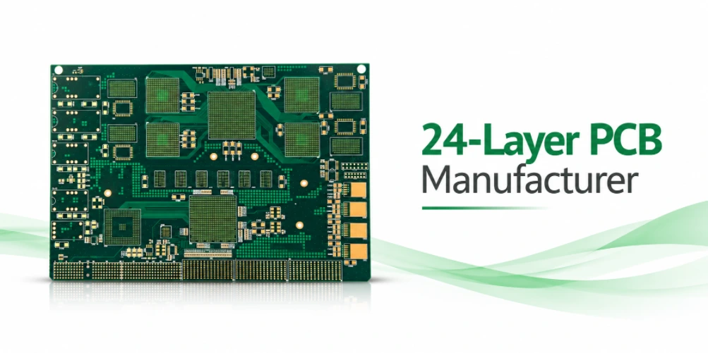
Yes—Highleap Electronics manufactures custom 24-layer PCBs. Our published rigid-board manufacturing range extends to 60 layers. For OEMs, engineering teams and procurement specialists, we provide an integrated route from 24-layer stack-up and DFM review through fabrication, inspection and optional PCB assembly.
Whether your project is a high-speed network board, compute or server platform, industrial controller or high-density instrumentation PCB, our team can review the actual build requirements—not just the layer count. We work with international buyers, including engineering and purchasing teams in Europe and Israel, who need a capable Chinese PCB manufacturing partner with clear technical communication.
Send Gerber or ODB++ data, your stack-up and target quantity. If the construction is not final, send the proposed stack-up and tell us which electrical or mechanical requirements are fixed.
The above are general published process capabilities, not a promise that every limit can be combined on the same 24-layer design. Final feasibility, tolerance and delivery are confirmed against your fabrication data.
Can Highleap Manufacture Your 24-Layer PCB? Yes.
Highleap is a PCB fabrication and electronics assembly manufacturer in China. A 24-layer rigid PCB sits within our publicly stated multilayer capability. We support prototype evaluation, new-product introduction and planned production volumes, with the required process route determined by the design.
We do not treat all 24-layer boards as interchangeable. A conventional through-hole construction, a low-loss 112G-class signal-integrity design and a board with multiple sequential-lamination cycles do not have the same process risk or cost. Our first job is to resolve those differences before the purchase order and production release.
Send us an existing 24-layer data package for quotation, or involve us while the stack-up is still open for a feasibility review. If the design calls for HDI, backdrilling, via-in-pad or hybrid high-frequency materials, identify those features at RFQ stage.
24-Layer PCB Manufacturing Capabilities: The Numbers Buyers Need
These figures are taken from Highleap's published rigid PCB capability table. They describe the manufacturing platform; they are ne blanket guarantees for every 24-layer stack-up. Achievable line width, finished hole, aspect ratio, board thickness and impedance tolerance must be reviewed together.
| Parametr | Publikovaná schopnost Highleap | What to specify on your 24-layer RFQ |
|---|---|---|
| Rigid-board layer count | Až 60 vrstev | 24-layer order, stack-up revision, total finished thickness |
| Inner / outer minimum trace & space | 2/2 mil (approx. 50/50 µm) | Critical layer-specific geometry and copper weights |
| Minimální mechanická vrtačka | 0.15 mm (published drill value) | Finished plated hole, drill size, tolerance, via aspect ratio |
| Minimální laserová vrtačka | 0.075 mm (published drill value) | Microvia layer pairs, pad dimensions, stacking and filling |
| Mechanical drilling aspect ratio | Až 20: 1 | Thickness-to-hole relationship and plated-barrel requirements |
| General rigid PCB thickness range | 0.2 – 8.0 mm | Actual 24-layer thickness and allowed tolerance |
| Řízená impedance | Published values: ±5 Ω at ≤50 Ω, or ±7% above 50 Ω | Single-ended / differential targets, reference layers, coupon method |
| Dostupné povrchové úpravy | Includes ENIG, ENEPIG, immersion silver, immersion tin, OSP and others | Finish choice, thickness, solderability and shelf-life requirements |
Naše širší high-frequency PCB capability includes low-loss and hybrid material constructions, while Výroba HDI PCB supports complex interconnect requirements. For Rogers, Isola, Megtron or other specified laminates, the exact grade, thickness, copper foil and stock position should be confirmed rather than assumed.
Engineering Controls That Decide Whether a 24-Layer Build Succeeds
Experienced buyers already understand the purpose of a multilayer PCB. The purchasing decision turns on whether the manufacturer can maintain the approved electrical and mechanical construction across the first article and repeated production lots. These are the principal checkpoints we discuss before fabrication release.
01 · Stack-up, resin flow and lamination
We review the 24-layer order, cores/prepregs, copper distribution, finished thickness and registration-sensitive features. Symmetry and copper balance matter, but so do specific material properties and lamination cycles. Any recommended dielectric or laminate substitution must be reviewed against the design's electrical requirements before approval.
02 · Controlled impedance and signal loss
Provide impedance targets and tolerance by layer/net class, reference-plane mapping, laminate loss requirements and any insertion-loss criteria. We can discuss coupon location and measurement scope, copper roughness and trace-geometry compensation. For high-speed serial interfaces, via-transition design and residual stub targets should be made explicit.
03 · Via structures and backdrilling
Drill strategy drives both yield and cost. Through holes, blind/buried vias, laser microvias, via-in-pad plated over and controlled-depth backdrills require different process steps. Specify start/stop layers, finished-hole sizes, fill/cap requirements, permitted stub lengths and drill-to-copper clearances. Complex stacked microvias must be confirmed against a proposed build sequence.
04 · Layer alignment and copper registration
Critical annular rings, plane antipads, fine-pitch escape patterns and backdrill clearances need coordinated checks. The practical drill-to-copper margin after lamination and plating is more relevant than a nominal CAD clearance viewed in isolation. We flag high-risk combinations before tooling release.
05 · Fabrication test and acceptance evidence
Highleap lists AOI and electrical testing in its company capability information. Depending on the agreed product class and purchase specification, an inspection plan may include impedance coupons, microsections, plating checks and additional reports. State the acceptance standard and required documentation at RFQ—not after the batch has shipped.
06 · Revision control and repeat orders
A production-ready package ties the fabrication drawing, stack-up, Gerber/ODB++ layers, drill maps, approved materials, impedance data and purchase-order revision together. When an ECO changes the laminate, drill or layer geometry, the new quotation and process route should reference the revised package.
Pro návrhy s použitím via filling and plating, specify capped-via appearance and flatness where BGA assembly requires it. If your layout is still being finalized, sharing the intended stack-up and drill map early can avoid a costly fabrication respin.
24-Layer PCB Programs We Are Structured to Evaluate
Our multilayer, high-frequency and assembly services are relevant to complex systems where routing density and electrical control are procurement requirements. Examples of project categories to discuss with our engineers include:
Product category does not replace design review. We qualify the manufacturability of the specific board, including reliability and acceptance requirements, rather than claiming every 24-layer application is a standard build.

A China 24-Layer PCB Manufacturing Partner for Europe and Israel
Engineering organizations in Germany, France, the UK, the Netherlands, the Nordic countries and Israel often have demanding qualification, documentation and change-control requirements. Highleap serves international PCB and PCBA projects and offers a manufacturing route in China for teams that want technical depth, competitive sourcing and a coordinated supplier relationship.
For European and Israeli OEMs, the practical reasons to evaluate Highleap are:
- Direct engineering discussion: stack-up feasibility, non-standard vias, impedance, materials and DFM questions can be discussed before committing to tooling.
- One supplier path: fabricate the 24-layer bare board and, when required, coordinate component procurement and SMT / montáž do průchozího otvoru under an agreed project scope.
- Documentation-based qualification: identify the IPC acceptance class, process/test records, material declarations, traceability requirements and any customer-specific quality clauses in the PO.
- Obchodní srozumitelnost: compare prototype, pilot and production quantities against tooling, materials, test scope, freight terms and total landed cost—rather than comparing bare-board unit price alone.
- Koordinace exportu: agree shipping destination, delivery terms and required paperwork before dispatch. For EU supply chains, specify required RoHS/REACH evidence and the exact applicable materials.
Highleap's company profile publicly lists quality-management certifications including ISO 9001, ISO 13485 and IATF 16949. Professional sourcing teams should request the current certificate copies, validity and relevant site/process scope as part of supplier approval. We do not present a certification listing as automatic approval of every product or regulatory regime.
Evaluating a supplier from Israel or Europe?
Tell us your country, intended destination, acceptance class, desired incoterm, current program phase and whether design-data confidentiality requires an NDA before file transfer. We can address these requirements during the RFQ and commercial review.
Discuss your 24-layer PCB requirement with Highleap →24-Layer PCB Fabrication and PCB Assembly from One Manufacturing Partner
A 24-layer bare board is only one stage of the product. Highleap also offers component sourcing, SMT, through-hole assembly, BGA-related inspection options, electrical/functional test arrangements, conformal coating and finished-product services. Combining fabrication and assembly planning helps engineering and procurement teams align board finishes, via-in-pad requirements, panelization, component availability and test access before the first build.
Bare 24-layer PCB fabrication
- Material and stack-up review
- Drill, HDI and impedance feasibility
- Fabrication, inspection and electrical test
- Prototype, pilot and volume RFQs
24-layer board + PCBA program
- BOM / approved-alternative review
- SMT and through-hole assembly planning
- Assembly inspection and agreed functional tests
- Single coordinated fabrication-to-assembly schedule
Assembly capabilities and inspection methods depend on package type, board dimensions, selected components and agreed test specifications.
Request a Serious 24-Layer PCB Quotation, Not a Generic Price Estimate
The two largest sources of quotation uncertainty are an incomplete stack-up and ambiguous special processes. A professional RFQ enables a manufacturer to quote the correct material and process route—and lets your sourcing team compare suppliers on equivalent technical scope.
| Send at RFQ stage | Why it changes price, risk or lead time |
|---|---|
| Gerber / ODB++ / IPC-2581, NC drill, fabrication drawing, revision | Geometry, drill structure, manufacturing constraints and controlled revision |
| Full 24-layer stack-up or proposed construction | Core/prepreg plan, copper weights, laminate procurement and lamination process |
| Target impedance, tolerance, frequency/loss requirement, coupon notes | Material choice, geometry compensation, validation method and cost |
| Via map: through, blind, buried, VIPPO, backdrill | Drilling, plating, sequential lamination, filling and test complexity |
| Finished thickness, outline, finish, acceptance class, test reports | Manufacturing tolerances, inspection scope and acceptance obligations |
| Prototype / pilot / production quantities, target date, destination | Tooling, panelization, material allocation, schedule and freight planning |
| If assembled: BOM, CPL, assembly drawing and test plan | Component availability, process suitability and complete PCBA quotation |
What determines 24-layer PCB cost? Board dimensions and yield per panel, material system, copper thickness, hole aspect ratio, sequential-lamination steps, controlled impedance, backdrilling, surface finish, test coverage, order size and delivery requirements. Two boards with 24 layers can have very different costs. An arbitrary “price per 24-layer board” without construction data is not a reliable procurement benchmark.
What determines lead time? Laminate stock, drilling and lamination process complexity, production load, qualification/test requirements and shipping arrangements. We quote the build against the actual file package; no fixed delivery promise applies to every 24-layer design.
From RFQ to Repeatable Production
- Submit your dataUpload design files, the stack-up, quantity, timing and quality requirements.
- Inženýrský přezkumResolve DFM questions, laminate and via constraints, inspection scope and assumptions.
- Schválit sestaveníConfirm specification, price, schedule and manufacturing revision before release.
- Fabricate & deliverProduce and inspect against the agreed package; coordinate assembly if required.
24-Layer PCB Manufacturer: Procurement FAQs
Does Highleap actually manufacture 24-layer PCBs?
Yes. Highleap publishes rigid multilayer capability up to 60 layers, which includes 24-layer builds. Approval of a particular design depends on the stack-up, materials, finished thickness, vias and required tolerances.
Can you support controlled impedance, HDI and backdrilling on a 24-layer PCB?
These processes are included in Highleap's published high-speed, rigid-PCB and HDI service offerings. Supply the impedance table, drill map, backdrill target and laminate requirements so the engineering team can confirm the combined build.
Can Highleap support a prototype first and then volume production?
Highleap offers prototype and production manufacturing. A pilot lot can be defined for stack-up, process and assembly validation before moving to the approved volume revision. Quantity, material availability and inspection scope affect the schedule.
Can your team handle PCB assembly as well as 24-layer board fabrication?
Yes. Highleap offers bare-board fabrication plus PCB assembly and component sourcing services. Include the BOM, placement files and test plan if you want a combined PCBA quotation.
Can we source from Highleap for a project in Europe or Israel?
Highleap works with international customers. State the destination and your documentation, quality, import and delivery-term requirements in the RFQ. Specific export documentation and shipping terms should be confirmed for the order.
What if our 24-layer stack-up is still under development?
Send the proposed layer build, required finished thickness, impedance targets, material preferences and via transitions. Mark fixed requirements versus design options. The engineering review can identify changes that need electrical approval before the layout is released.

doporučené příspěvky
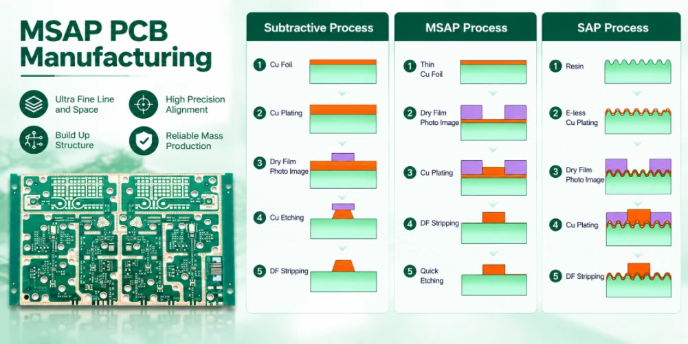
Výroba desek plošných spojů mSAP pro jemné obvody
Highleap Electronics poskytuje mSAP PCB výrobu...
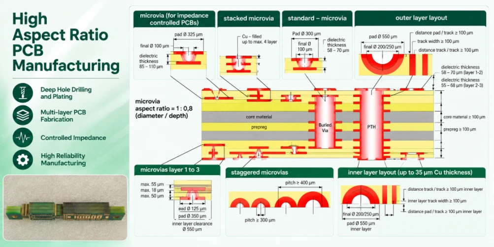
Výroba desek plošných spojů s vysokým poměrem stran pro pokovené průchozí otvory
Highleap Electronics dodává desky plošných spojů s vysokým poměrem stran...
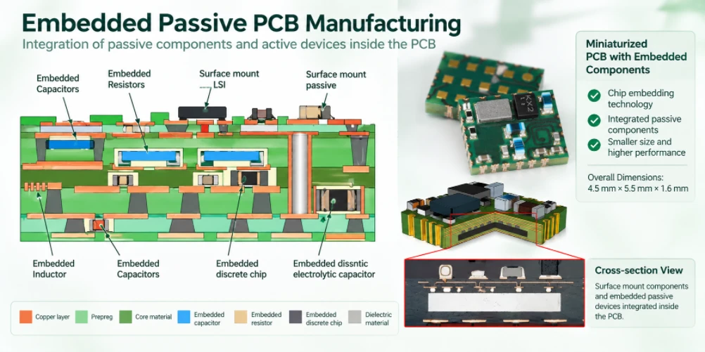
Výroba pasivních desek plošných spojů pro integrované návrhy
Highleap Electronics dodává pasivní desky plošných spojů...
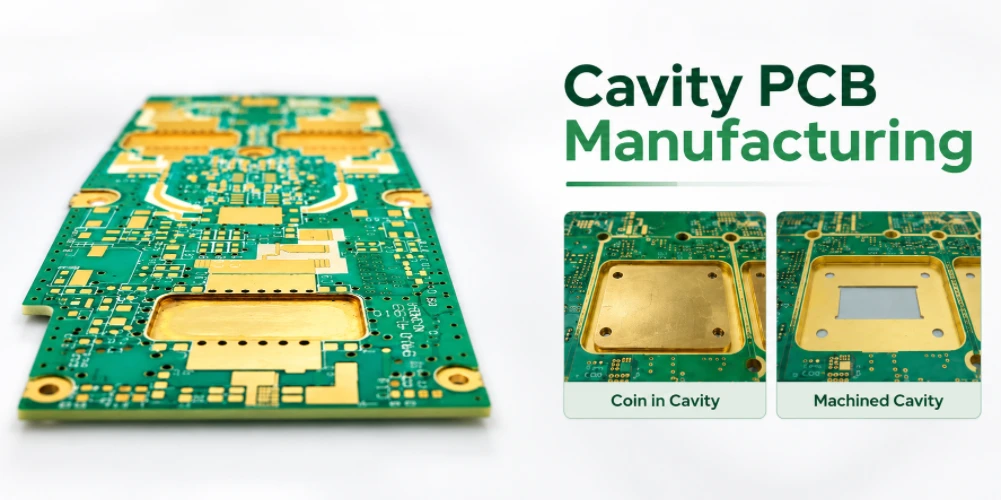
Výroba dutinových desek plošných spojů pro návrhy přesných desek
Dutinová deska plošných spojů je účelově vyrobená deska se zapuštěným nebo...
Jak získat cenovou nabídku na desky plošných spojů
Provedeme pro vás analýzu DFM/DFA a ozveme se vám se zprávou. Své soubory můžete bezpečně nahrát prostřednictvím našich webových stránek. Pro vypracování cenové nabídky potřebujeme následující informace:
-
- Gerber, ODB++ nebo .pcb, spec.
- Seznam kusovníků, pokud požadujete montáž
- Množství
- Čas otáčení
Kromě výroby desek plošných spojů nabízíme komplexní škálu elektronických služeb, včetně návrhu desek plošných spojů, výroby desek plošných spojů a komplexních řešení. Ať už potřebujete pomoc s prototypováním, ověřováním návrhu, zajištěním zdrojů součástek nebo hromadnou výrobou, poskytujeme komplexní podporu, abychom zajistili úspěch vašeho projektu.
Pro služby PCBA prosím poskytněte kusovník (BOM) a případné konkrétní montážní pokyny. Nabízíme také analýzy DFM/DFA pro optimalizaci vašich návrhů z hlediska vyrobitelnosti a montáže a zajištění plynulého výrobního procesu.