
IT-601G PCB Manufacturing for Multilayer and HDI Boards
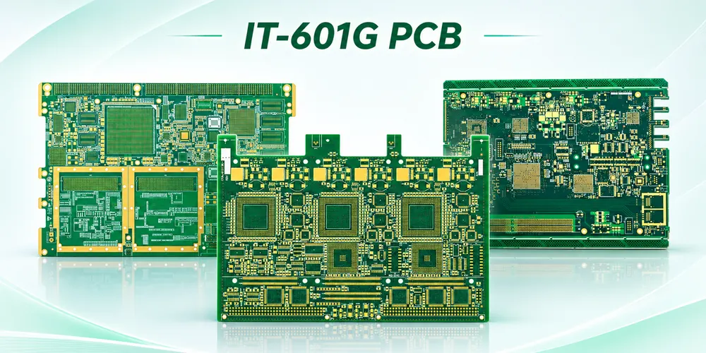
Illustration of dense PCB routing for an HDI build.
ITEQ IT-601G is a halogen-free, high-Tg material system for advanced HDI PCBs that need low through-thickness expansion and lower dielectric loss. The grade-specific datasheet reports 1.1% Z-axis expansion from 50°C to 260°C. It also reports a 230°C Tg by DMA and a 210°C Tg by TMA. For stacked microvias, the release decision still depends on the construction and on evidence from the actual interconnect sequence.
Resolve conflicting IT-601G values before simulation
Online material summaries can show 10 GHz Dk and Df as 3.5 and 0.0060 at 50% resin content, or label 230°C as a TMA result. For the model and purchase specification, record the grade, document number, revision, resin content, frequency and method together. The ITEQ IT-601G grade sheet W-CTE-1002-64D, Rev. 1.0-26 describes the following specimen results. Do not reconcile differing sources by averaging their values or by moving Dk and Df from one row to another.
| Vlastnictví | Hlášený výsledek | Method or construction |
|---|---|---|
| Dk / Df při 1 GHz | 3.5 / 0.0055 | 70% obsah pryskyřice; IPC-TM-650 2.5.5.9 |
| Dk / Df při 10 GHz | 3.28 / 0.0064 | 70% obsah pryskyřice; IPC-TM-650 2.5.5.13 |
| Tg | 230°C DMA; 210°C TMA | IPC-TM-650 2.4.24.4 and 2.4.24, respectively |
| Rozšíření osy Z | 1.1 % od 50 °C do 260 °C | IPC-TM-650 2.4.24; laminátový vzorek |
| Td / T260 / T288 | 420°C / >60 min / >60 min | Td at 5% mass loss; T-times measured separately |
Použijte IT-601GTC a IT-601GBS to identify the copper-clad laminate and prepreg in the material record. For an impedance or loss model, ask for construction-specific inputs for the actual glass style, pressed dielectric and copper foil. Keep the model and coupon on that same revision. A 70% resin-content datasheet value can be valid and still be the wrong input for a layer with a different construction.
Plan evidence before each lamination hides an interface
IT-601G’s reported Z-axis expansion is useful for screening where temperature excursions load the vertical interconnects. In a stacked via column, however, each copper connection depends on its own geometry, target preparation and plating. A low-expansion laminate does not prevent a weak interface from opening. A staggered transition trades routing area for the ability to avoid placing the next via directly on the previous filled via. Check whether the package can escape with that arrangement before committing to a stacked column.
Hypothetical 2+N+2 process review. In this example two build-up layers are added symmetrically on either side of a central multilayer structure. Some signals pass through a buried via in the center, then through two laser microvias on one side. The checkpoints below describe what to agree for this example; they are neither a claim about a Highleap production line nor a universal process traveler.
| Fáze výstavby | Risk to close | Evidence to define with the fabricator |
|---|---|---|
| Central subassembly | Buried-hole barrel or land defects become hard to isolate after build-up. | Register the inner layers and define representative checks of buried span, plating and any required fill before it is covered. |
| First build-up pair | Poor contact to the target, incomplete fill or a recessed fill surface under the next via. | Agree on local pressed thickness, pad capture, fill profile and planarity inspection at sites that represent the next landing. |
| Second build-up pair | Misregistration or weak copper interfaces within the stacked path. | Section representative stack geometry and define a continuity coupon with each interface included in the measured path. |
| Qualification and release | Intermittent opens during temperature excursions; integration errors at fine-pitch lands. | Agree on thermal exposure and resistance monitoring, board net test, and finished land/assembly inspection as distinct requirements. |
An electrical coupon that bypasses the longest or most demanding stack answers the wrong question. Retain the panel or coupon identity through stress and sectioning so failed locations can be compared to geometry. A section at ambient temperature can look acceptable at the sampled plane even when an interface opens only while hot. For sekvenční laminace, decide which observations need to occur during fabrication and which can be made on the completed structure. The IPC-TM-650 method index provides test references; use the method, conditioning and limits specified for the actual program.
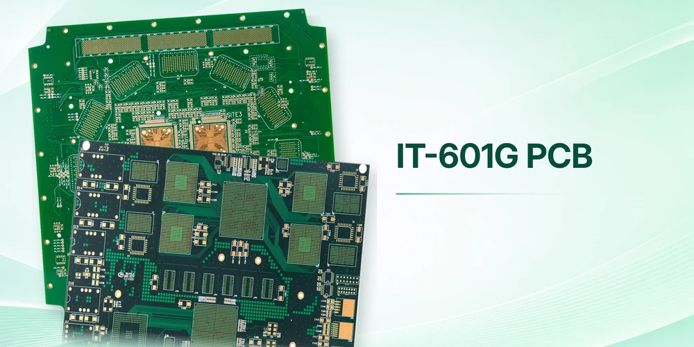
HDI PCB illustration. Artwork does not establish the buried interconnect construction or reliability.
Put copper foil changes under revision control
The ITEQ sheet lists 18 µm RTF and RTF2 low-profile foils and 18 µm HTE standard-profile foil with separate peel-strength results. Those are not roughness specifications. Two foil constructions at the same thickness can differ in adhesion treatment and conductor loss. For loss-sensitive layers, specify the permitted foil and the surface information required by the model. Keep the test coupon on the same layer construction as the routed traces.
A foil or prepreg substitution can change more than one result. The new bonding package can change the final dielectric spacing and laser depth, while a new foil treatment can change electrical loss without a large change in TDR impedance. Record proposed substitutions against four items: the pressed thickness, landing and fill geometry, impedance and loss inputs, and the qualification evidence. If any has changed, identify which requirement needs to be demonstrated again. This connects ovládání impedance with the process route instead of treating the two as independent drawing approvals.
VÝROBA A MONTÁŽ DESEK PLOŠNÝCH PLOŠIN
Planning an IT-601G PCB build?
Highleap může společně posoudit požadavky na konstrukci a montáž desky.
Include the via map, lamination sequence and the qualification requirements for buried interfaces.
Release the HDI stack and the assembly together
Memory, SiP and other compact devices can force via-in-pad and place limits on board and package coplanarity. Agree on pad finish and solder-mask registration, and verify that the released drawings address via fill, cap and flatness where solder joints sit above vias. Include panel handling in the assembly review. X-ray can aid hidden solder-joint inspection; bare-board coupons and sections remain necessary when the acceptance plan requires evidence of buried interconnect integrity.
Pro IT-601G fabrication and PCBA estimate, provide the controlled material revision, core and prepreg constructions, via span and stack maps, foil and electrical inputs, and coupon acceptance requirements. Pair those files with the package footprints, BOM, placement file and assembly drawing. Highleap Electronics can then review material sourcing, the build-up sequence, and the first-article inspection scope against one release package.

O autorovi
Charles L.
Výrobní inženýr a CAM pro plošné spoje ve společnosti Highleap Electronics
Karel má více než 10 let zkušeností v oblasti CAM inženýrství desek plošných spojů a výroby elektroniky, specializuje se na ověřování souborů desek plošných spojů, DFM analýzu a přípravu výroby vícevrstvých, HDI, RF a vysokorychlostních desek. Díky znalosti Genesis, InCAM a CAM350 zajišťuje přesná data, stabilní procesy a vysokou produktivitu výroby.
Ve společnosti Highleap Electronics se zaměřuje na optimalizaci procesů a hodnocení vyrobitelnosti, aby pomohl zákazníkům snížit rizika, zkrátit dodací lhůty a dosáhnout spolehlivých výrobních výsledků.

doporučené příspěvky
Sestavení desek IT-602G HDI pro SSD disky a paměťové moduly
Příklady desek plošných spojů IT-602G pro HDI, SSD a paměťové moduly...
Desky plošných spojů IT-988GL s propojovací deskou a řízením procesů s nízkým CTE
Výroba vícevrstvých desek plošných spojů IT-988GL...
Deska plošných spojů Arlon 85NT: Výroba polyimidu a SMT řízení
Ilustrace výroby desek plošných spojů; druh materiálu a...
Výroba vysoce kvalitních desek plošných spojů Arlon 33N
Ilustrace výroby desek plošných spojů. Potvrďte zadané...
Jak získat cenovou nabídku na desky plošných spojů
Provedeme pro vás analýzu DFM/DFA a ozveme se vám se zprávou. Své soubory můžete bezpečně nahrát prostřednictvím našich webových stránek. Pro vypracování cenové nabídky potřebujeme následující informace:
-
- Gerber, ODB++ nebo .pcb, spec.
- Seznam kusovníků, pokud požadujete montáž
- Množství
- Čas otáčení
Kromě výroby desek plošných spojů nabízíme komplexní škálu elektronických služeb, včetně návrhu desek plošných spojů, výroby desek plošných spojů a komplexních řešení. Ať už potřebujete pomoc s prototypováním, ověřováním návrhu, zajištěním zdrojů součástek nebo hromadnou výrobou, poskytujeme komplexní podporu, abychom zajistili úspěch vašeho projektu.
Pro služby PCBA prosím poskytněte kusovník (BOM) a případné konkrétní montážní pokyny. Nabízíme také analýzy DFM/DFA pro optimalizaci vašich návrhů z hlediska vyrobitelnosti a montáže a zajištění plynulého výrobního procesu.