
Služby výroby a montáže desek plošných spojů
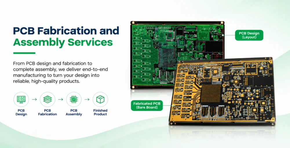
Highleap Electronics provides PCB fabrication and assembly services for OEMs that want custom bare boards and populated PCBAs supplied through one coordinated manufacturing project. Our service scope includes multilayer PCB manufacturing, HDI, rigid-flex, heavy-copper and metal-core PCB options, together with SMT/through-hole assembly, agreed component sourcing, inspection and project-specific tests. Fabrication and assembly are reviewed against the same approved board, BOM and acceptance package.
For a new electronics product, the PCB construction and the component package cannot always be quoted independently. A BGA escape pattern may determine whether HDI or filled vias are required; a power board may need heavy copper and a different soldering approach; a flex circuit may need carriers and stiffeners during SMT. Highleap coordinates these details before production so the manufactured board is appropriate for the assembly the OEM intends to receive.
One-Stop PCB Fabrication and Assembly Services
Highleap can manufacture the bare PCB and coordinate subsequent component assembly under one approved order, with fabrication and assembly responsibilities defined for the project. Jedno custom printed circuit board manufacturing scope covers material selection to the released drawing, drilling, plating, etching, solder mask, surface finish and bare-board verification. Our PCB population and assembly operations cover the approved components, SMT/THT work and agreed post-assembly inspection or tests.
This service is relevant for OEMs that currently purchase bare boards from one supplier and place them with a separate electronics assembler. Coordinating both stages can reduce ambiguity around stencil apertures, BGA land patterns, board thickness, connector fit, panel rails and test access. Highleap’s PCB fabrication and PCBA operations are managed as one commercial project; their specific production locations should be confirmed rather than assumed to be in the same building.
A production order may contain a main controller PCB, display PCB, sensor daughterboard and communication board, each with different constructions and component populations. Those assemblies can be scheduled as a matched set when the OEM specifies the correct revisions, connector pairing, firmware and shipment configuration. Highleap manufactures to that release rather than silently reconciling conflicting files.
The exact scope can end at electrically tested bare boards, at inspected populated assemblies or at an agreed electromechanical subassembly. Special environmental qualification, certification, calibration and test-fixture development should be named in the RFQ and not inferred from the phrase “one-stop service.”
Multilayer PCB Fabrication and SMT PCB Assembly
Highleap supports multilayer PCB fabrication with SMT assembly for embedded controllers, network hardware, data-acquisition boards, industrial communication products and other dense electronics. A multilayer printed circuit board build may include controlled impedance, ground/power planes, high-speed signal layers and mechanical features that affect subsequent SMT processing.
Projects can include 4-layer IoT and sensor boards, 6- or 8-layer industrial controller PCBAs, 10- or 12-layer network and communication modules, and more complex embedded computing assemblies. The required layer count belongs to the customer’s electrical and mechanical design; it does not by itself determine assembly capability or reliability. Fine-pitch packages, component access, thermal pads, via placement and board finish are equally important when the populated board is quoted.
For BGA processors, DDR memory or high-speed communication interfaces, the fabrication drawing should define stack-up, finished copper, controlled-impedance targets and any specific via treatment. The assembly release should match that board revision and specify package identities, placements, stencil requirements and the inspection plan. A 100-ohm differential impedance coupon test can support the PCB manufacturing evidence, but it cannot replace Ethernet link, processor boot or system-level functional tests.
In mixed SMT/THT products such as an industrial gateway with large connectors, through-hole soldering and mechanical fit should be considered during multilayer board design. A board designed solely around SMT panel efficiency may need different breakaway supports or insertion access once pluggable terminal blocks and shielded connectors are added.
HDI PCB Fabrication with Fine-Pitch BGA Assembly
HDI PCB fabrication and assembly are relevant when fine-pitch components, compact board dimensions or routing density require laser microvias, blind/buried structures or via-in-pad designs. Highleap může zkontrolovat high-density interconnect PCB fabrication together with the assembly plan for processor boards, compact RF modules, cameras, industrial vision hardware, wearables and miniaturized controllers.
A 0.4 mm-pitch BGA can require different escape routing from a larger BGA. Where vias are placed directly in solder pads, the specified filling, capping and planarization affect paste printing and solder-joint behavior. Sequential lamination and multiple microvia levels may also affect cost and schedule. These details should be settled during DFM, not after an expensive HDI panel has been fabricated.
The assembly scope may include high-density BGA placement, fine-pitch QFN/LGA devices, miniature passives and double-sided reflow. The solder-paste design, component moisture sensitivity, board flatness and inspection method are evaluated from the actual packages. Hidden-joint X-ray can be specified where appropriate; visible AOI alone cannot assess every connection beneath a BGA.
For an OEM developing a high-density wireless gateway or industrial compute module, quote the bare board and assembly using the same footprint revision. This helps determine whether an issue belongs to the land pattern, fabrication detail, stencil process or component condition rather than passing the problem between suppliers.
Rigid-Flex PCB Fabrication and Assembly Services
Highleap can evaluate rigid-flex PCB fabrication and populated assembly for compact electronic products with components on rigid sections and flexible interconnect regions. Náš rigid-flex PCB assembly services are relevant to camera modules, wearable electronics, sensors, small medical or measurement devices, vehicle electronics and space-constrained industrial instruments, subject to project-specific engineering approval.
The bare-board drawing must distinguish layer construction in rigid and flex areas, coverlay openings, stiffeners, rigid-to-flex transitions and the intended bend region. Bending conditions are not the same for a one-time static installation and a repeated dynamic flex application. The OEM should identify permitted bend radii and assembly/final-installation restrictions from the design’s qualified construction rather than assuming all flexible regions may be folded after reflow.
During assembly, temporary carriers or fixtures may be required for print, placement, reflow, depaneling and test. Component keep-outs near bend transitions, connector reinforcement and support under populated areas should be reviewed before tooling. A rigid-flex PCB can reduce the number of cables and connectors in the finished product, but only when mechanical design, fabrication and soldering instructions are aligned.
For multiple small flex tails or delicate connectors, the final packing and handling instructions are part of the manufacturing scope. A completed PCBA should arrive without being forced into an unapproved fold or attachment position just to reduce shipping volume.
Heavy Copper and Aluminum PCB Fabrication with Assembly
Heavy copper and metal-core PCB assembly require the bare-board current/thermal design and the soldering process to be reviewed together. Highleap can assess heavy-copper PCB fabrication with component assembly for industrial motor controls, EV charging interface electronics, inverter and energy-storage controllers, DC/DC converters and power distribution boards.
The specified copper weight must be considered with trace width, spacing, plated features, current path, allowed temperature rise and connection hardware. Heavy copper alone does not guarantee a current rating independent of board geometry and cooling. Large power terminals, MOSFETs, relays and magnetics may have substantially different thermal mass from the fine-pitch control ICs on the same PCBA. Stencil, soldering and inspection methods should account for both regions.
Highleap může také zkontrolovat aluminum-substrate and metal-core PCB manufacturing for LED lighting, high-power LED drivers and other thermal-management electronics. A metal-core board can support thermal spreading according to the qualified construction, but the thermal dielectric, heatsink interface, solderable pads and mechanical mounting still determine product performance. A completed LED PCBA may need additional optical and thermal testing beyond standard solder-joint inspection.
| Custom PCB construction | Typical populated electronics | Assembly-related specification |
|---|---|---|
| Vícevrstvá deska plošných spojů | Industrial controller and network PCBAs | Stack-up, SMT package mix, signal and mechanical interfaces |
| HDI microvia PCB | Dense processor, RF and sensor modules | Via-in-pad, BGA footprints, flatness and hidden-joint inspection |
| Pevná ohebná deska plošných spojů | Camera and compact instrument PCBAs | Bend limits, stiffeners, carriers and final handling |
| Těžká měděná deska plošných spojů | Power control, charging and motor electronics | Current/thermal geometry and high-mass solder joints |
| Aluminum metal-core PCB | LED modules and thermal power assemblies | Dielectric insulation and heatsink/assembly interfaces |
Turnkey PCB Fabrication, Component Sourcing and DFM
Highleap can coordinate PCB fabrication, purchased components and assembly as a turnkey order when the OEM provides the approved design and purchasing instructions. This arrangement is useful for multi-board industrial electronics, network appliances, EV charging controllers, wireless modules and embedded systems that need a supplier to manage board and component readiness together.
Jedno PCB and PCBA design-for-manufacturing review compares the bare-board construction with the selected packages, assembly drawings and any tests. Potential issues include pad/footprint conflicts, solder-mask openings, panel clearance, wrong component height, via-in-pad details, inaccessible test pads or incompatible finish/handling requirements. Such findings should be approved by the design owner before manufacturing files are changed.
A turnkey purchase can be full BOM sourcing, partial turnkey or assembly with customer-supplied material. Approved manufacturer part numbers, alternatives, no-substitution items and component ownership should be defined per BOM line. Where the product has multiple PCBA revisions or optional fitted variants, the manufacturing package should provide a clear matrix identifying what is built and how each assembly is labeled and tested.
For cost planning, PCB fabrication and the sourced BOM may proceed on related but distinct schedules. The production-ready date depends on the material with the longest procurement requirement, correct bare boards, assembly tooling and any needed test fixture. A single supplier simplifies coordination, but it does not remove genuine component shortages or external qualification steps.
PCB Fabrication and Assembly Testing and Quality Control
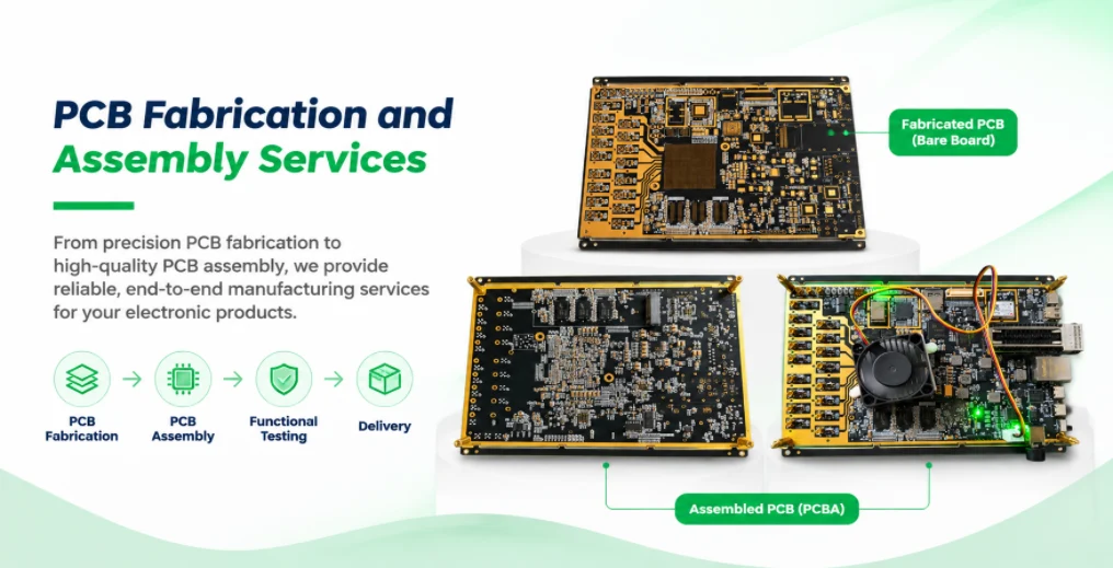
Bare PCB quality control and assembled PCBA verification are different deliverables and should be quoted separately when the customer needs both sets of evidence. Highleap's PCB fabrication quality and inspection services can be included alongside assembly inspection and functional testing, with the applicable acceptance criteria, report format and sampling defined by the project.
At the bare-board stage, electrical netlist testing checks copper continuity and isolation, while dimensional, plating and other inspections address relevant fabrication workmanship. For controlled-impedance designs, agreed coupons or measurement methods may be required. At the populated-board stage, first-article checks establish component configuration; AOI evaluates visible soldering and placement features, and X-ray can support inspection of BGAs and other hidden joints.
A functional test is then required when the customer needs evidence that the actual assembled circuit behaves as intended. A network gateway may need programmed firmware and interface checks; an industrial controller may require channel-by-channel I/O; an LED driver may need specified electrical and thermal conditions. None of those is demonstrated solely by a bare-board open/short test or a visual AOI pass.
For repeat orders, agree the customer quality class and standard revision, traceability requirements, testing frequency, disposition of failures and delivered records. EMC, environmental cycling, safety compliance and special RF characterization are separate qualification activities unless they are specifically included in the agreement.
Custom PCB Fabrication and Assembly Quote
Highleap can provide a project-specific quote for custom PCB fabrication and assembly from the complete released PCB and PCBA data. The quotation can separate bare-board fabrication, components, SMT/THT assembly, tooling, inspections, programming, optional finishes and test work. PCB complexity, material availability, component sourcing and quantity all affect cost and lead time.
Files required for a combined PCB and PCBA quotation
- Holá deska plošných spojů: Gerber/ODB++ or equivalent, drill files, fabrication drawing, material and stack-up, copper, finish, mechanical features and impedance requirements.
- Součásti: complete BOM with reference designators, quantities, exact MPNs, DNP positions, approved alternates and consignment details.
- Shromáždění: CPL/centroid, assembly drawings, connector/hardware specifications, board variants and soldering/handling restrictions.
- Ověřování: workmanship criteria, inspection/test procedures, firmware, calibration data, fixtures and traceability requirements.
- Komerční: quantities for prototype and production, forecast, packaging, destination and requested release dates.
Can Highleap make HDI or rigid-flex boards and populate them? Highleap can evaluate fabrication and assembly for those custom constructions using the actual files, stack-up and component data. Special tooling and acceptance requirements must be confirmed for each design.
Does one-stop fabrication and assembly include component purchasing? It can. Full turnkey, partial turnkey or customer-consigned sourcing is agreed during RFQ review, and the quote identifies which materials and operations are included.
Highleap Electronics — Custom PCB Fabrication & PCBA Manufacturing
Send your board manufacturing data, BOM, assembly drawings, quantities and testing requirements. Highleap can review the bare-board construction and populated assembly together and prepare one coordinated manufacturing proposal.

doporučené příspěvky

Sestavení plošných spojů síťového přepínače: Testování Ethernetu, PoE a portů
Osazování desek plošných spojů síťových přepínačů ve společnosti Highleap Electronics přináší...

Sestava plošných spojů výkonové elektroniky pro systémy s vysokým proudem a převodem energie
Highleap Electronics dodává desky plošných spojů pro výkonovou elektroniku...

Osazování automobilové elektroniky na plošných spojích: Sledovatelnost a řízení procesů
Highleap Electronics vyrábí desky plošných spojů a dodává...
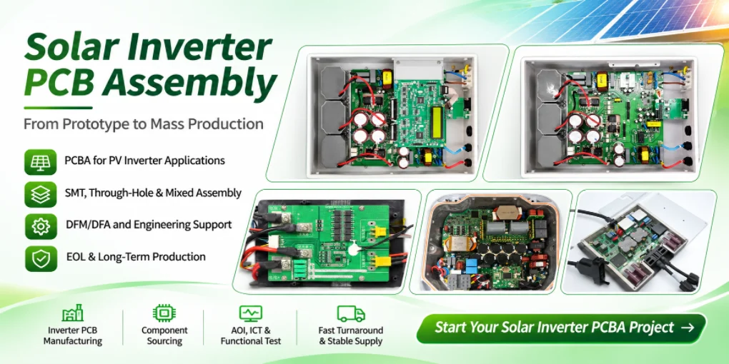
Sestava desky plošných spojů solárního invertoru pro napájecí a řídicí desky
Pokud sháníte desku plošných spojů pro solární invertory, Highleap...
Jak získat cenovou nabídku na desky plošných spojů
Provedeme pro vás analýzu DFM/DFA a ozveme se vám se zprávou. Své soubory můžete bezpečně nahrát prostřednictvím našich webových stránek. Pro vypracování cenové nabídky potřebujeme následující informace:
-
- Gerber, ODB++ nebo .pcb, spec.
- Seznam kusovníků, pokud požadujete montáž
- Množství
- Čas otáčení
Kromě výroby desek plošných spojů nabízíme komplexní škálu elektronických služeb, včetně návrhu desek plošných spojů, výroby desek plošných spojů a komplexních řešení. Ať už potřebujete pomoc s prototypováním, ověřováním návrhu, zajištěním zdrojů součástek nebo hromadnou výrobou, poskytujeme komplexní podporu, abychom zajistili úspěch vašeho projektu.
Pro služby PCBA prosím poskytněte kusovník (BOM) a případné konkrétní montážní pokyny. Nabízíme také analýzy DFM/DFA pro optimalizaci vašich návrhů z hlediska vyrobitelnosti a montáže a zajištění plynulého výrobního procesu.