
中国8层HDI PCB制造商
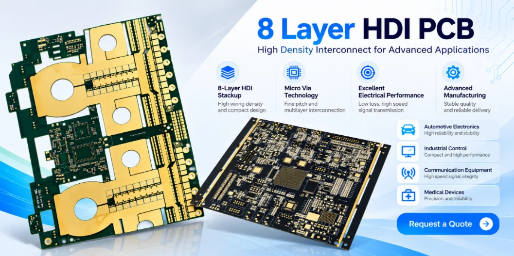
Highleap Electronics 提供 8 layer HDI PCB manufacturing for electronic products requiring high-density routing, microvia interconnections, fine-pitch BGA breakout and complex multilayer construction. We review the actual stackup, via architecture, materials and special fabrication requirements to establish a suitable manufacturing route. Submit your Gerber or ODB++ files for engineering review and a project-specific quotation, with PCB assembly available for integrated manufacturing projects.
An eight-layer HDI PCB is not defined by copper-layer count alone. The buildup structure, microvia connections, drilling and plating requirements, conductor geometry, surface finish and mechanical features all influence manufacturing feasibility, cost and lead time. Highleap evaluates these requirements as one integrated PCB design rather than treating each special feature as an isolated option.
目录
Have an 8 Layer HDI PCB Project?
Send your stackup, fabrication files, via specifications and order quantity for manufacturing review and quotation.
8 Layer HDI PCB Manufacturing Capabilities
Highleap Electronics reviews custom eight-layer HDI PCB projects involving dense component routing, laser-drilled microvias, blind and buried vias, fine-pitch BGA connections and demanding electrical or mechanical specifications. The appropriate process depends on the complete fabrication package, including layer arrangement, via connections, material selection, board dimensions and required tolerances.
Depending on the design, the manufacturing review may cover the following requirements:
- HDI结构: 1+6+1 and 2+4+2 buildup concepts, sequential lamination, blind and buried vias, stacked or staggered microvias, and via-in-pad structures.
- Fine-pitch routing: BGA and CSP escape routing, small capture pads, fine trace and spacing requirements, and controlled registration between layers.
- Via filling and capping: Specified resin-filled or copper-filled vias, planarized surfaces and copper-capped via-in-pad structures where required by the design.
- Special mechanical features: Complex board outlines, plated slots, castellated holes, plated edges, controlled-depth routing, cavities and precision mounting features.
- Electrical and material requirements: Controlled impedance, high-speed or RF layouts, low-loss dielectric materials, mixed copper weights and thermal-via structures.
- Surface finish and assembly interfaces: ENIG, ENEPIG or other specified compatible finishes, selective contact plating, solder-mask openings and component assembly requirements.
These are engineering requirements to evaluate, not a guarantee that every option can be combined on every eight-layer stackup. For example, a design requiring stacked microvias, copper-filled via-in-pad and selective hard gold needs a compatible process sequence that protects both the interconnections and the final component pads.
For general multilayer production information, see 8层PCB制造. For HDI projects, the additional via architecture and special processing must be included in the fabrication specification.
Stackup and HDI Engineering Requirements
The stackup determines how the eight copper layers are interconnected, how much routing space is available and which lamination and drilling processes are required. The choice between 1+6+1, 2+4+2 or another qualified arrangement should be based on component pitch, routing congestion, electrical requirements, via reliability and manufacturing feasibility.
1+6+1 buildup places one buildup layer on each side of a six-layer central structure. It may suit designs whose routing density can be handled with a more limited buildup arrangement. A 2+4+2 buildup provides additional buildup layers on each side, potentially creating more routing transitions but also introducing additional lamination, drilling, filling and registration requirements. Neither structure is universally better; the correct choice depends on the design.
The engineering review should establish the following before production:
- Layer and dielectric definition: Copper-layer sequence, core and prepreg construction, dielectric thicknesses, copper weights and finished board thickness.
- Via connection map: Start and end layers for each via type, microvia spans, blind or buried connections, and stacked or staggered arrangements.
- Microvia details: Laser opening, capture-pad geometry, target-pad interface, filling method and copper capping requirements.
- Fine-line manufacturability: Minimum trace width and spacing, annular rings, pad dimensions and layer-to-layer registration requirements.
- 电气性能: Controlled-impedance targets, reference-plane continuity, critical signal transitions and any high-speed or RF requirements.
- Materials and mechanical features: Laminate grade, thermal requirements, board profile, plated edges, special holes and any controlled-depth machining.
Via filling, plugging and copper capping are not interchangeable specifications. For fine-pitch BGA designs, the required pad surface and via structure must be stated clearly. Likewise, a controlled-impedance target should be reviewed against the actual dielectric construction, conductor geometry, copper and material characteristics rather than an assumed nominal stackup.
Highleap的 PCB DFM审查 can help identify fabrication conflicts and clarify open engineering requirements before production release. If your project requires a rigid-flex construction rather than a rigid HDI board, refer to our separate 8层软硬结合板 manufacturing page.
8 LAYER HDI PCB MANUFACTURING
Get a Quote for Your 8 Layer HDI PCB
Need an 8 layer HDI PCB manufacturer? Send your fabrication files, stackup, microvia specifications and order quantity to Highleap Electronics for a project-specific manufacturing review and quotation.
Pricing and lead time confirmed after engineering review.
8 Layer HDI PCB Cost and Lead Time
一个的成本 8层HDI PCB depends on its manufacturing route, not simply the board dimensions or number of copper layers. Additional buildup stages, laser drilling, microvia filling, copper capping, fine-line processing and specialized materials can change the production requirements. Special edge plating, castellated holes, cavities, selective finishes and controlled-impedance requirements may also affect tooling, process sequence and inspection.
The following factors are particularly important when preparing a quotation:
- HDI buildup: Number of sequential lamination stages and the complexity of the layer-to-layer connection map.
- Via processing: Microvia quantity and arrangement, blind or buried vias, filling, capping and any required reliability evaluation.
- Design density: Minimum trace and spacing, fine-pitch component pads, registration tolerances and expected manufacturing yield.
- Materials and copper: Laminate grade, dielectric thickness, copper weights, finished thickness and any qualified hybrid construction.
- Mechanical and finishing requirements: Board size, profile tolerances, plated features, surface finish and special machining.
- Quantity and inspection: Prototype or production volume, panelization, electrical testing, documentation and additional acceptance criteria.
Lead time is assessed against material availability, the approved process sequence, order quantity, production capacity and the required inspection scope. More complex buildup structures or specialized materials may affect the schedule. A delivery estimate should therefore be confirmed against the actual design and order requirements.
For a general pricing reference, see 8层PCB成本. That resource addresses eight-layer PCB pricing more broadly; an HDI quotation must additionally account for the specified microvias, buildup construction and special processing.
To compare supplier quotations accurately, provide the same fabrication data, stackup, via definitions, material requirements, surface finish, order quantity and testing criteria. Comparing prices based only on the phrase “8 layer HDI PCB” may result in different manufacturing assumptions and non-equivalent offers.
Manufacturing Quality and Inspection
Quality control for an eight-layer HDI PCB should reflect the construction and its critical features. A typical process may include inner-layer imaging and inspection, lamination, laser microvia processing, plating or filling, mechanical drilling, outer-layer imaging, solder mask, surface finish, profiling and electrical testing. The actual sequence varies according to the buildup structure and specified special processes.
Inspection requirements may include:
- 层完整性: Inner-layer pattern inspection, registration, copper clearance and dimensional verification.
- Microvia and hole quality: Via geometry, plating condition, microsection analysis and inspection of critical via interfaces where specified.
- 已填充并封盖的过孔: Fill integrity, surface planarity and suitability for the intended component-pad construction.
- 电气性能: Continuity and isolation testing, plus impedance verification using agreed test structures where required.
- 特殊功能: Inspection of plated edges, castellated holes, machined profiles, cavities or selective finishes according to the drawing.
- Acceptance documentation: Applicable IPC specifications and revision, acceptance class, test reports and customer-specific requirements.
Stacked microvias and other critical interconnections may require additional qualification beyond routine final electrical testing. Acceptance criteria should be agreed before production rather than assumed after fabrication. Any proposed changes to the approved stackup, materials, via structure or functional geometry should be reviewed with the customer.
For projects requiring both bare-board fabrication and component assembly, Highleap also provides PCB组装服务. Assembly requirements such as fine-pitch BGA placement, soldering, inspection and testing should be included in the project scope when applicable.
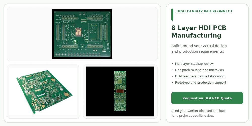
RFQ Requirements and PCB Manufacturing Quote
To obtain a meaningful quotation for an 8 layer HDI PCB manufactured in China, provide the latest available design files and identify any special processes that are essential to the finished board. The more clearly the construction and acceptance requirements are defined, the easier it is to evaluate manufacturability, process scope and delivery feasibility.
- 制造文件: Gerber X2 or ODB++, drill files, board outline and fabrication drawing.
- 堆叠: Eight copper layers, laminate grade, dielectric thicknesses, copper weights and finished board thickness.
- HDI connections: Via map, microvia spans, blind or buried vias, stacked or staggered structures, and filling or capping requirements.
- 临界几何: Minimum trace and spacing, fine-pitch pads, board dimensions, hole tolerances and mechanical profile requirements.
- 特殊工艺: Controlled impedance, low-loss materials, plated edges, castellated holes, cavities, selective finishes or other nonstandard features.
- 质量要求: Applicable IPC specification, acceptance class, electrical testing, inspection reports and additional qualification needs.
- 订单详细信息: Prototype or production quantity, target delivery date and packaging or shipping requirements.
- 程序集范围: BOM, pick-and-place data, assembly drawings and testing requirements if PCBA is required.
If the stackup or via structure is still under development, identify the unresolved items in your inquiry. Engineering review can then focus on those decisions before the final manufacturing specification is approved. Special processes should be evaluated as a combined construction; their compatibility cannot be established from a list of individual features alone.
Request an 8 Layer HDI PCB Manufacturing Quote
Send your fabrication files, stackup, via specifications, order quantity and delivery requirements for a project-specific manufacturing review.

推荐文章
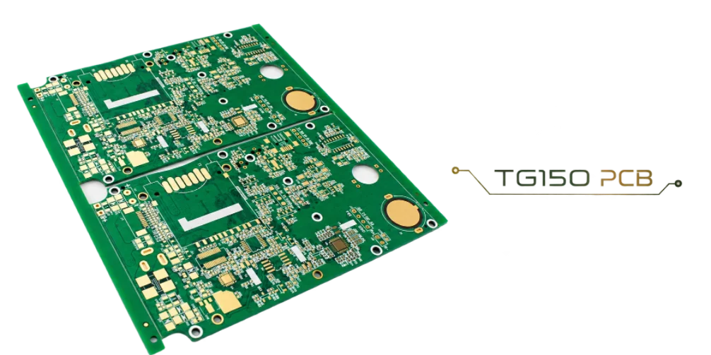
TG150 PCB制造商,提供制造和组装服务
Highleap Electronics 生产 TG150 PCB 板……
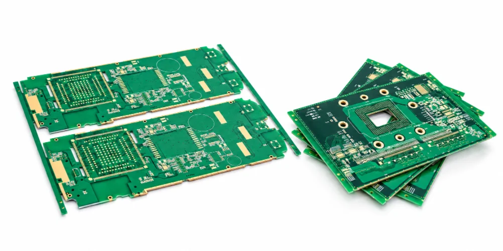
TG140 PCB材料选择与制造
目录 TG140 PCB材料及选型...
如何为定制电路板选择TG180 PCB材料
选择Tg180 PCB不仅仅是选择一个……
服务器主板PCB制造与组装
服务器主板PCB制造正变得越来越……
如何获取 PCB 报价
我们将为您进行DFM/DFA分析,并尽快向您提供报告。您可以通过我们的网站安全上传文件。为了给您报价,我们需要以下信息:
-
- Gerber、ODB++ 或 .pcb,规格。
- 如果需要组装,请提供 BOM 清单
- 数量
- 转弯时间
如需 PCBA 服务,请提供您的 BOM(物料清单)和任何具体的装配说明。我们还提供 DFM/DFA 分析,以优化您的设计,提高可制造性和装配性,确保生产流程顺畅。