
Výrobce desek plošných spojů Taconic TSM-DS3 pro tepelně stabilní vícevrstvé RF systémy
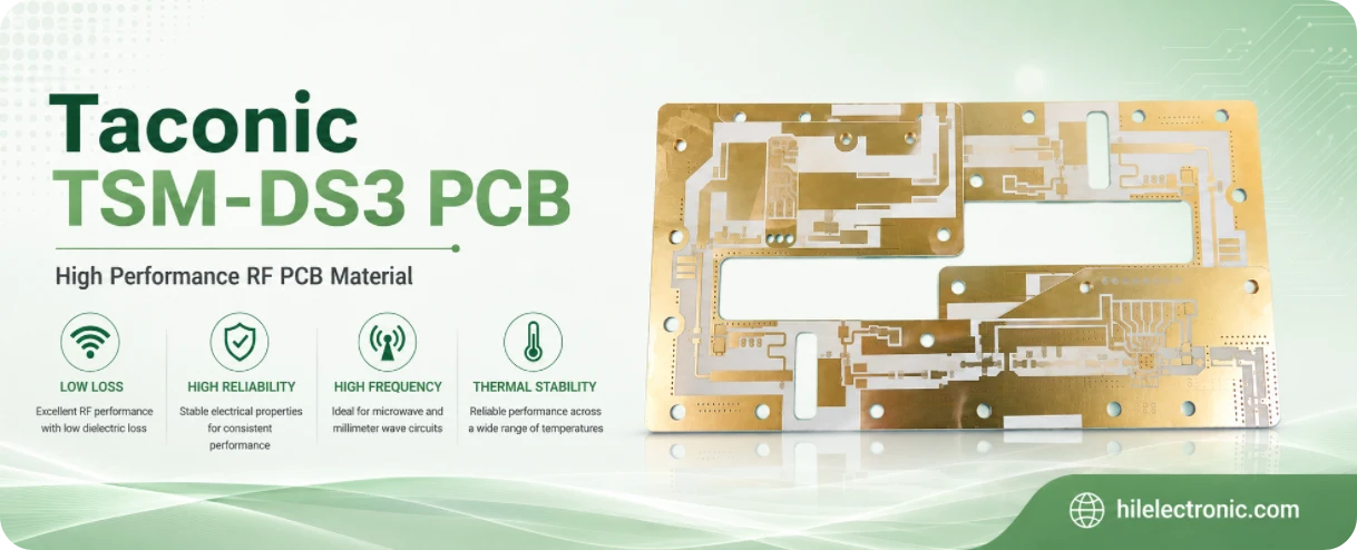
Společnost Highleap Electronics vyrábí a montuje desky plošných spojů Taconic TSM-DS3 pro radary, fázované anténní soustavy, ATE, zesilovače, filtry, letecké a kosmické rádiové systémy a velkoformátové vícevrstvé obvody. Cenová nabídka se zaměřuje na kompletní konstrukci – jádra TSM-DS3, spojovací materiál, lisovanou tloušťku, registraci, vrtání, pokovování, vzorky, montáž a environmentální přijatelnost – nikoli pouze na datový list laminátu.
Vícevrstvý sestavovací osciloskop TSM-DS3 od Highleap
Highleap podporuje nízkoztrátové vícevrstvé RF struktury postavené pomocí TSM-DS3, včetně PTFE nebo hybridních konstrukcí, řízené impedance, sekvenční laminace, hustých propojovacích struktur a pokročilých propojovacích struktur mezi vrstvami při kontrole kompletního propojení. Velké panely, neobvyklé spojovací linie, tenké dielektrické rozteče a kritická registrace z hlediska RF jsou hodnoceny spíše než s obecným grafem vlastností.
Důležité: Sestavení TSM-DS3 lze podporovat od technických vzorků a kvalifikačních šarží až po opakovanou výrobu. Projekty s náročnými tepelnými, fázovými, spolehlivostními nebo propojovacími požadavky procházejí procesní kontrolou před potvrzením konečné výrobní trasy.
Nejlépe sedí
Teplotně citlivé radarové a fázované anténní soustavy, desky rozhraní ATE, vysokofrekvenční signály s vysokým počtem vrstev, filtry, zesilovače a letecká elektronika.
Hlavní chyba
Zacházení se stabilním laminátem jako se zárukou stabilního výkonu produktu bez definování mědi, spojů, teplotních gradientů, krytu, montáže a testování.
Rozsah výroby
Ověřování materiálů, konstrukce skládání a spojovacích linií, zpracování PTFE, škálování, řízená impedance, prostupy, montáž a kvalifikace definovaná zákazníkem.
Vstupní nabídky
Detaily jádra/prepregu, tloušťka lisovaného materiálu, RF a teplotní limity, přes strukturu, rozměry, množství, montážní balení a plán zkoušek.
Kdy je TSM-DS3 lepším RF materiálem
Taconic TSM-DS3 je nízkoztrátový, keramicky plněný PTFE laminát s malým množstvím výztuže ze skelných vláken. Společnost AGC uvádí nominální Dk 3.0 ± 0.05, tepelnou vodivost přibližně 0.65 W/m·K a klade důraz na dielektrickou stabilitu v závislosti na teplotě. Jeho komerční hodnota nespočívá pouze v „nízkých ztrátách“. Je to kombinace předvídatelnosti pro vysokofrekvenční záření, tepelného chování, výztuže a vhodnosti pro více vrstev.
Zvolte TSM-DS3, když
- fáze, impedance nebo rezonance musí zůstat předvídatelné v závislosti na teplotě;
- deska plošných spojů je velká, má vysoký počet vrstev nebo je mechanicky náročná;
- výkon radaru, fázovaného anténního soustavy, zesilovače, filtru nebo akustické technologie (ATE) závisí na opakovatelné dielektrické vzdálenosti;
- lze kvalifikovat kompatibilní systém propojení s nízkými ztrátami.
Zvolte jiný materiál, když
- Primárním cílem je co nejnižší Dk pro účinnost antény;
- běžná FR-4 nebo termosetová nízkoztrátová třída již splňuje environmentální a kanálové požadavky;
- návrh nemá definovaný požadavek na teplotu ani fázi;
- Zákazník nemůže schválit kompletní konstrukci jádra/prepregu.
TSM-DS3 se často stává cenným poté, co konstruktér identifikuje systémový problém – teplotně závislou fázi, nestabilní rezonanci, registraci na velkém panelu nebo obtížnou vícevrstvou RF strukturu – a to nejen proto, že produkt pracuje na vysoké frekvenci.
Výrobní kapacity pro vícevrstvé systémy TSM-DS3
Společnost Highleap dokáže posoudit pevné RF desky, vícevrstvé konstrukce TSM-DS3 a hybridní stacky. Projekty mohou zahrnovat fastRise 27 nebo jiný schválený spojovací materiál, sekvenční laminaci, pokovování průchozích otvorů, slepé nebo laserem vrtané struktury, řízenou impedanci a montáž na klíč. Každá položka je ověřena oproti skutečnému návrhu; žádná generická stránka s materiály nemůže stanovit proveditelný počet vrstev nebo strukturu propojení.
| Výrobní oblast | Recenze inženýrství Highleap | Vyžadováno rozhodnutí zákazníka |
|---|---|---|
| Jádro a spojovací linie | Zkontrolujte tloušťku jádra TSM-DS3, měď, spojovací materiál, počet vrstev, tloušťku lisování, spotřebu pryskyřice a symetrii. | Schválit konečné uspořádání a veškeré změny konstrukce, které lze zakoupit. |
| Škálování a registrace panelu | Naplánujte pohyb materiálu, vyvážení mědi, cíle nástrojů, sekvenci laminace a registraci vrstev po vrstvě. | Identifikujte kritické RF zarovnání, dutiny, pole, konektory a mechanické vztažné body. |
| Vrtání a pokovování | Definujte aktivaci PTFE, trasu vrtání, měď na stěně otvoru, poměr stran, fáze vyplňování otvorů nebo mikrootvorů a odběr vzorků průřezu. | Zajistěte prostřednictvím třídy spolehlivosti a jakýchkoli požadavků na tepelný cyklus nebo IST. |
| VF ovládání | Modelujte impedanci ze skutečné konstrukce a plánované fáze, rezonátoru, vložného útlumu nebo podle specifických kuponů zákazníka. | Uveďte parametr přijetí, frekvenci, toleranci a zkušební metodu. |
| Montáž | Projděte si konektory s vysokou hmotností, stínění, tepelná rozhraní, reflow, podporu desek, čištění a přístup k testům. | Poskytněte kusovník, mechanický výkres, zkušební přípravek a požadavky na prostředí. |
Lze nabídnout prototypovou, nízkosériovou a opakovanou výrobu. Přechod na sériovou výrobu vyžaduje identifikaci zmrazeného materiálu, konstrukci lisu, data o měřítku a kritéria pro uvolnění; jinak se každá šarže stává novým experimentem.
Konstrukční požadavky pro teplotně stabilní VF výkon
Fráze „teplotně stabilní laminát“ nedefinuje výkon produktu. Odezvu desky ovlivňuje také roztažnost mědi, napětí v pouzdře, pájené spoje, konektory, součástky, proudění vzduchu a rozložení tepla. Výzva k nabídkovému řízení (RFC) proto musí převést požadavky na prostředí do měřitelných kritérií pro desku nebo produkt.
Zajistěte tyto elektrické a tepelné vstupy
- rozsah provozních a skladovacích teplot;
- povolená změna impedance, fáze, zpoždění, rezonance nebo vloženého útlumu v závislosti na teplotě;
- frekvenční rozsah, úroveň výkonu, pracovní cyklus a místní zdroje tepla;
- referenční rovina, konektor, anténa a kalibrační struktury;
- tepelná rozhraní, kovové nosiče, rozvaděče tepla, montážní moment a omezení krytu;
- požadovaný tepelný cyklus, šokový test, test zahoření nebo funkční test;
- korelace kupónu a produktu a metoda deembeddingu zákazníka.
Společnost Highleap může vyrábět splňující tyto požadavky, ale kvalifikace VF a tepelných parametrů na úrovni systému zůstává společným inženýrským úkolem. Výsledek měření impedance holé desky při pokojové teplotě sám o sobě nedokáže prokázat výkon fázovaného pole v celém provozním rozsahu.
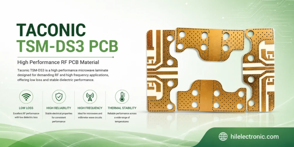
Stavba TSM-DS3 s fastRise 27 nebo jinými spojovacími materiály
U vícevrstvé RF desky plošných spojů je vytvrzená spojovací linie elektrickou vrstvou. Její tloušťka se vytváří během laminace a závisí na konstrukci prepregu, procentuálním podílu mědi, topografii, tlaku, teplotě, vakuu, velikosti panelu a toku pryskyřice. Tloušťka surového plechu není zaručenou konečnou dielektrickou vzdáleností.
- Potvrďte kompatibilitu. Ověřte vybraný spojovací materiál s povrchy TSM-DS3, úpravou mědi, cyklem vytvrzování, teplotním průběhem a přilehlými materiály.
- Zmapujte poptávku po pryskyřicích. Zkontrolujte hustotu mědi, velké čisté plochy, dutiny, oblasti výplní a výšku lokálních prvků.
- Stanovte si cílové hodnoty tloušťky stlačeného materiálu. Použijte dostupné konstrukce vrstev a výrobní data, nikoli idealizovanou nominální hodnotu.
- Naplánujte postupnou laminaci. Počítejte každý lisovací cyklus a kumulativní tepelnou expozici jader, pokovených prvků a mikrootvorů.
- Ovládejte dimenzionální pohyb. Aplikujte cíle škálování a registrace na základě kompletního tiskového balíčku.
- Korelační kupóny. Ujistěte se, že kupón obsahuje stejné materiály, měď, lisovací cyklus a pokovování jako funkční obvod.
Více informací naleznete v příručce Highleap pro návrh prepregů fastRise 27 a RF via.
Aplikace: Co materiál řeší v produktu
Elektronika s fázovaným polem a radarová elektronika
Výkon pole závisí na fázové konzistenci, opakovatelné geometrii napájení, teplotním chování a registraci napříč velkým panelem. TSM-DS3 dokáže tyto požadavky splnit, pokud zákazník také řídí geometrii prvků, konektory, radom, kalibraci a teplotní gradienty na úrovni produktu.
Rozhraní ATE a struktury sondy a karty
Velká velikost desky, vysoký počet vrstev, husté propojování, řízená impedance, mechanická rovinnost a tepelné cykly se mohou vyskytovat společně. Návrh by měl stanovit, které rozměry a elektrické cesty řídí přesnost přípravku; použití úzkých tolerancí všude zbytečně zvyšuje náklady.
Zesilovače, filtry a letecký a kosmický RF
Nízké ztráty a teplotní stabilita mohou snížit drift, ale hustota výkonu, uzemnění, spolehlivost pokovených otvorů, mechanická montáž a čistota sestavy zůstávají kritické. Laminát je jednou ze součástí plánu regulace.
Velkoformátové RF vícevrstvé
Výztuž a chování materiálu mohou unést rozměrově náročné konstrukce, ale vyvážení mědi, pořadí lisování, škálování panelů, vrtání a montážní podpora musí být navrženy specificky pro danou velikost desky.
Faktory nákladů a dodací lhůty
| Faktor | Proč je to důležité | Obchodní kontrola |
|---|---|---|
| Konstrukce jádra/prepregu | Neobvyklé tloušťky, více vrstev nebo speciální spojovací fólie ovlivňují nákup a kvalifikaci lisu. | Schválit dostupné stavby včas. |
| Počet vrstev a cykly lisování | Více cyklů zvyšuje registraci, vyplňování pryskyřicí, spolehlivost propojení a rozměrové riziko. | Použijte minimální architekturu, která splňuje požadavky na směrování a izolaci. |
| Velikost desky a zarovnání RF | Velké panely vyžadují měření, podepření, kontrolu rovinnosti a další kontrolu. | Definujte kritické vztažné body a realistické tolerance. |
| Slepé průchodky a mikroprůchodky | Laserové vrtání, vyplňování, sekvenční laminace a kupóny na spolehlivost přidávají procesní kroky. | Používejte HDI pouze tam, kde to vyžaduje průraz nebo RF přechod. |
| Kvalifikace teploty/RF | Environmentální komory, přípravky, kalibrace, analýza dat a opakované vzorky zvyšují náklady a harmonogram. | Definujte přesný plán akceptační zkoušky a vzorkování. |
| Složitost montáže | Velké desky BGA, lisovací konektory, stínění, nosiče a tepelná rozhraní mohou dominovat celkovým nákladům na desky plošných spojů. | Odešlete montážní a mechanické údaje s poptávkou na holou desku. |
Pro přesnou konstrukci je nutné zkontrolovat dodací lhůtu materiálu a minimální objednané množství. Highleap nenabídne zdánlivě rychlý prototyp s použitím jednoho stacku a tiše nepřesune výrobu na jiný.
Co je třeba předložit k cenové nabídce TSM-DS3
Uveďte přesný stupeň TSM-DS3 a tloušťku jádra, typ a hmotnost mědi, spojovací materiál, plné propojení, cílové hodnoty tloušťky po stlačení, tabulku impedance, frekvenční rozsah, fázové nebo ztrátové limity, provozní teplotu, architekturu propojení, kritické registrační rozměry, velikost desky a panelu, povrchovou úpravu, množství, prognózu, cílové hodnoty dodání a požadavky na kvalitu/testy.
Pro montáž přidejte kusovník, těžiště, výkresy, podrobnosti o konektoru a stínění, tepelná rozhraní, limity pro přetavování a čištění, povrchovou úpravu, přístup k testům, informace o upínacím přípravku, profil prostředí a očekávání ohledně reportingu.
Užitečným výstupem z Highleapu je balíček pro rozhodnutí o výrobě: dostupnost materiálu, navrhované složení materiálu, problémy s vyrobitelností, požadovaná schválení zákazníkem, postup procesu, důkazy o kontrolách/zkouškách, faktory ovlivňující náklady a rizika spojená s dodací lhůtou. To je to, co kupující potřebuje k rozhodnutí, zda továrna může produkt vyrobit.
Obchodní Často kladené otázky
Může Highleap vyrobit vícevrstvou desku plošných spojů Taconic TSM-DS3?
Ano, vhodné vícevrstvé a hybridní projekty TSM-DS3 lze posoudit. Konečná proveditelnost závisí na spojovacím materiálu, tloušťce lisovaného materiálu, počtu vrstev, rozměrech, architektuře via, registraci, montáži a požadavcích na testování.
Je TSM-DS3 lepší než TLY-5?
Ne obecně. TSM-DS3 se často volí pro teplotní stabilitu a předvídatelnost více vrstev; TLY-5 je atraktivní pro antény s velmi nízkým Dk a nízkými ztrátami nebo pro milimetrové vlnové struktury. Vyberte podle požadavků na produkt, nikoli podle jednoduchého pořadí.
Lze použít fastRise 27 jako spojovací materiál?
Může být vhodný pro validované konstrukce, ale pro kompletní souhrn je nutné zkontrolovat kompatibilitu, počet vrstev, spotřebu pryskyřice, tloušťku lisování, cyklus lisování a kumulativní tepelnou historii.
Jaké testy lze zahrnout?
V závislosti na projektu může cenová nabídka zahrnovat elektrické zkoušky, kontrolu kritických rozměrů, mikroskopické řezy, impedanční zkoušky, rezonátorové nebo fázové vzorky, tepelné cykly, AOI/rentgenové měření, funkční zkoušky nebo zákazníkem definované RF testy.
Jak se určuje cena?
Cena závisí na materiálu konstrukce, velikosti desky, počtu vrstev, lisovacích cyklech, struktuře propojení, kritických tolerancích, množství, složitosti montáže a požadovaných radiofrekvenčních nebo environmentálních důkazech. Pro pevnou cenovou nabídku zašlete kompletní datový balíček.

doporučené příspěvky

Taconic RF 35 vs. RO4350B DPS
ObsahRF-35 vs. RO4350B Zadávání veřejných zakázek a...

Výroba desek plošných spojů filtrů TMM4
Výroba plošných spojů filtrů TMM4 je řízena...

Výroba desek plošných spojů TMM6
Výroba TMM6 je stránka pro řízení procesu pro středně těžký...

Výroba desek plošných spojů TMM3 pro RF moduly
Výroba desek plošných spojů TMM3 je nejužitečnější tam, kde RF modul...
Jak získat cenovou nabídku na desky plošných spojů
Provedeme pro vás analýzu DFM/DFA a ozveme se vám se zprávou. Své soubory můžete bezpečně nahrát prostřednictvím našich webových stránek. Pro vypracování cenové nabídky potřebujeme následující informace:
-
- Gerber, ODB++ nebo .pcb, spec.
- Seznam kusovníků, pokud požadujete montáž
- Množství
- Čas otáčení
Pro služby PCBA prosím poskytněte kusovník (BOM) a případné konkrétní montážní pokyny. Nabízíme také analýzy DFM/DFA pro optimalizaci vašich návrhů z hlediska vyrobitelnosti a montáže a zajištění plynulého výrobního procesu.