
Cartes de circuits imprimés de fond de panier IT-988GL avec contrôle de processus à faible coefficient de dilatation thermique
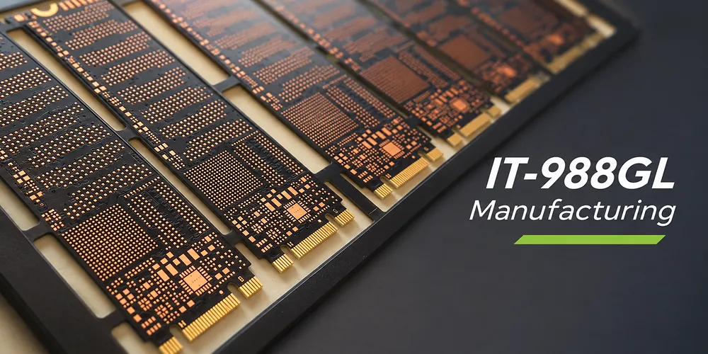
IT-988GL multilayer PCB manufacturing illustration.
Long-reach backplanes and high-speed switch boards place simultaneous demands on dielectric loss, dimensional stability and mechanical interfaces such as press-fit connectors and large BGAs. IT-988GL is an ITEQ low-loss, low-CTE laminate and prepreg option, but finished-board registration, warpage and channel performance depend on the complete stack-up and process. Highleap evaluates IT-988GL PCB fabrication and assembly packages by aligning material callouts, copper profile, plated-hole geometry and component-interface requirements.
ITEQ publishes IT-988GL 10 GHz Dk/Df of 3.21/0.0033 for a 70%-resin test specimen, together with 1.7% Z-axis expansion from 50°C to 260°C. The low dielectric-loss specification and low expansion are useful starting points; real channel loss and assembly reliability still depend on copper, geometry, plating and component attachment.
IT-988GL Electrical and Thermal Properties That Affect the Finished Board
ITEQ’s current IT-988GL supplier sheet reports a 10 GHz Dk of 3.21 and Df of 0.0033 sur un 70%-resin test specimen. On a 55%-resin specimen it gives Dk 3.63 and Df 0.0041 at the same frequency. These differences are material to impedance and loss calculations. A design using the 70%-resin Dk cannot assume that value applies to every core thickness or prepreg construction under the IT-988GL family name.
| ITEQ IT-988GL parameter | Supplier-published typical value | Pertinence en ingénierie |
|---|---|---|
| Dk / Df, 10 GHz, 70% resin specimen | 3.21/0.0033 | Useful low-loss design baseline for the stated sample |
| Dk / Df, 10 GHz, 55% resin specimen | 3.63/0.0041 | Demonstrates construction-dependent dielectric variation |
| Tg, TMA / DMA | 180 ° C / 200 ° C | The temperature test method matters in material comparisons |
| Expansion selon l'axe Z, 50–260 °C | 1.7 % | Input to plated-hole and multilayer thermal-fatigue review |
| X/Y CTE, 40–125°C | 8 / 9 ppm/°C, per one stated method | Relevant to in-plane dimensional stability, not a BGA life guarantee |
| Td, 5% mass loss | 400 ° C | Material decomposition threshold, not continuous-use temperature |
| Absorption d'humidité | 0.12 % | Supplier test result; storage and reflow handling remain process-specific |
The supplier identifies IT-988GLTC copper-clad laminate and IT-988GLBS prepreg. Material forms must be explicitly specified on the purchasing drawing, including copper profile and acceptable alternatives. Confusing IT-988GL with IT-988GLSE can alter both the dielectric values and the manufacturing construction; suffixes should not be treated as a formatting detail.
Une comparaison avec lower-expansion FR-4 constructions under defined test conditions can help establish whether a specialty low-CTE laminate is needed. Frequency, resin content, reinforcement and copper-foil assumptions should be matched wherever possible; a published property advantage does not translate directly into the same percentage improvement in a complete channel.
IT-988GL PCB manufacturing for low-loss switch and backplane designs
For a long data-center backplane channel, multilayer fabrication controls for server motherboard constructions must be reviewed alongside a buildable stack-up and channel-level loss target, not just a laminate designation.
For a detailed fabrication review, an approved stack-up or field-solver constraints, layer count, conductor finishes, drill or backdrill details and test-coupon requirements help confirm the build. Those engineering details can be supplied as the design matures; they are not all required to make an initial inquiry. A short description of the backplane or server board and its approximate quantity is enough to start the discussion.
Long-Channel Backplane PCB Manufacturing with IT-988GL
The resin-content basis changes the optimization problem
At 10 GHz the published 55%-resin sample Dk is 3.63, whereas the 70%-resin sample is 3.21. Choosing a higher-resin construction may also change the pressed dielectric thickness and the amount of glass in the electric field. That means a lower nominal Dk cannot simply be selected from a table while leaving trace width, spacing and layer thickness untouched. The field solver needs the buildable physical stack-up, and the fabricator needs to know which dielectric construction it is expected to produce.
For long channels, requirements often include a complete insertion-loss mask rather than a single-frequency limit. The mask must be linked to the actual channel and its test structures. Passing one dielectric-value check at 10 GHz does not guarantee attenuation performance across the frequency range of interest.
IT-988GL is attractive for applications with lengthy routed interconnects because low dielectric loss can help preserve channel margin. Nevertheless, total insertion loss includes conductor effects, trace geometry, vias and connectors. The higher the operating frequency, the more sensitive the result becomes to surface roughness and transitions in the return-current path.
The PCB copper roughness contribution is particularly important in a low-Df system. Reducing dielectric loss makes other contributors a larger share of the remaining budget. A coarse foil profile can erase some expected benefit of the laminate grade; very smooth foil may instead change mechanical adhesion and fabrication requirements. Copper treatment belongs in the approved bill of materials, not merely in a design engineer’s simulation notes.
Loss budgeting example—not a measured performance claim
Considérons deux hypothétique routing options with identical connector, via and foil geometry but different dielectric loss tangents. If the dielectric attenuation were proportional to Df within a limited model, changing from Df 0.0070 to 0.0033 would reduce only the modeled dielectric-loss term to approximately 47% of its previous value. It would not cut total channel loss by 53%, because conductor and discontinuity losses remain. This simplified example also ignores frequency dispersion and field distribution, so it must not be used to predict a real board’s dB performance.
The required specification is a channel budget by frequency, or another agreed signal-integrity criterion, with layer assignments and connectors identified. For long backplane PCBs, the connector footprint, drill pattern, antipads and stub control may need as much attention as the straight trace sections.
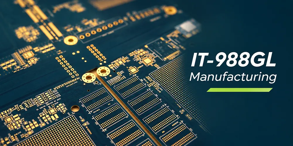
Fine-pitch pad and plated-hole details for the IT-988GL fabrication and assembly review.
Stack-Up and Layer Registration for Low-CTE IT-988GL Multilayer Boards
Low CTE does not eliminate local thermal mismatch
A low X/Y expansion number describes a material test specimen under defined conditions. Real boards contain copper-rich and copper-poor regions, resin layers and installed packages with different stiffness and thermal expansion. Local curvature can appear during solder reflow even when the laminate’s bulk in-plane CTE is relatively low. Board flatness and BGA behavior therefore require attention to copper balance, thickness symmetry and assembly layout, not merely a materials upgrade.
The effect of copper density and local heating on board flatness and warpage under assembly conditions should be reviewed against the finished outline, component distribution and support method.
Likewise, the supplier’s 1.7% Z-axis expansion is a useful comparison point but cannot determine whether a given plated hole survives the application’s temperature cycle. Critical barrels must be evaluated for geometry, plating and defects, particularly when a thick switch card experiences several assembly or rework excursions.
Low in-plane expansion supports dimensional stability but does not make registration automatic. Copper imbalance, core thickness, press sequencing and local density differences still affect how the stack moves and how much resin fills between etched features. The released construction should include dielectric thickness and reference-plane definitions in the approved stack-up together with the core/prepreg schedule and critical drill-to-copper registration tolerances.
Four items deserve particular attention in IT-988GL stack-up engineering:
- Géométrie d'impédance. Use actual 55%/70% construction-appropriate dielectric inputs, not a single Dk copied from a comparison table. Define layer-specific PCB impedance control tolerances and coupons.
- Conductor profile. Match foil roughness and etch compensation to the loss model; finished copper width differs from nominal CAD width.
- Fiber/resin homogeneity. On long, coupled channels, the PCB glass-weave effect can contribute skew and local impedance variation that an average Dk calculation hides.
- Via architecture. Thick boards can require careful review of aspect ratio, barrel copper and any backdrilling or stub-control details specified by the design owner.
The material’s published 1.7% Z-axis expansion is helpful context for plated-hole fatigue, but the finished hole’s mechanical behavior depends on copper plating, geometry and all fabrication thermal cycles. The inspection plan should include representative microsections and defined electrical tests for the construction being purchased.
PCB FABRICATION & ASSEMBLY
Planning an IT-988GL backplane or server PCB?
Highleap can discuss low-CTE construction, long-channel requirements and the BGA or connector assembly scope.
A first inquiry is simple. No complete fabrication or assembly package is needed to start. A short description of the backplane or server-board application and approximate quantity is enough; connector or BGA details are helpful if known.
What low in-plane CTE changes in a high-layer-count PCB
Low in-plane thermal expansion can reduce the nominal dimensional mismatch between the PCB and certain mounted packages, but it cannot cancel copper imbalance, glass-weave asymmetry, resin movement or local heating during reflow. The practical stack-up objective is repeatable layer registration and controlled board flatness, especially near large BGA footprints and dense connector fields.
Thermal-expansion figures also have direction and method: the material’s X/Y CTE should not be confused with its Z-axis expansion, which contributes to plated-hole strain. Microsection evidence, finished-hole geometry and defined thermal-stress tests remain necessary where through-hole reliability is critical.
Low-CTE Backplane PCB Assembly: BGA and Press-Fit Connectors
Server and networking assemblies bring additional stresses after bare-board fabrication. Large BGA packages impose thermomechanical loads as board and component materials expand at different rates. A laminate with lower in-plane CTE can reduce one part of that mismatch, but package dimensions, solder alloy, board thickness, copper distribution and the temperature-cycle envelope also affect solder-joint fatigue.
Pour ces plateformes, component placement, reflow and connector integration on server boards should be planned against the approved bare-board construction rather than treated as a separate downstream task.
Le solder-paste, stencil and reflow controls for fine-pitch BGA packages should be coordinated with the land pattern, solder-mask definition and board flatness. Hidden-joint inspection, reflow and rework planning depend on the package and the approved assembly process; no published IT-988GL number guarantees BGA fatigue life.
Where the package hides solder joints from optical inspection, radiographic inspection of hidden solder joints after assembly can be included according to package geometry and the agreed inspection plan.
| Interface | Common manufacturing or assembly risk | Preuve ou contrôle à demander |
|---|---|---|
| Long differential stripline | Insertion loss or skew exceeds the model | Representative impedance and loss coupons as specified |
| Dense press-fit connector zone | Finished hole tolerance and plating affect fit | Drill chart, copper thickness and approved press-fit requirements |
| Large BGA with dense via escape | Board warpage, local solder bridging or joint fatigue | Warpage/assembly checks and suitable hidden-joint inspection |
| Deep plated through-holes | Thermal cycling strains the barrel | Cross-section and project-defined reliability tests |
| Substitution matérielle | Dk/Df and thickness no longer match approved simulation | Formal stack-up and design-owner approval |
The correct quality plan distinguishes bare-board checks from product qualification. IPC-6012 and IPC-A-600 provide finished-board performance and acceptability frameworks when specified; separate system-level channel validation and assembly reliability testing may still be needed. Qualification tests for finished-board thermal and mechanical reliability should be selected according to the operating environment and customer acceptance criteria.
Backplane PCB assembly with press-fit connectors and large BGA packages
Press-fit connectors impose a finished-hole diameter and copper-plating requirement that differs from a soldered through-hole pin. Dense connector arrays can also make board flatness and local reinforcement important. Separately, a large BGA requires pad geometry, mask clearance and a soldering profile that can be inspected and reworked within the product’s constraints.
Le mechanical load created when press-fit contacts enter plated holes makes finished-hole diameter, plating and board support part of the mechanical assembly review.
For IT-988GL server or network assemblies, the fabrication drawing, connector manufacturer’s press-fit specification and assembly drawing should be reconciled before release. A completed bare-board electrical test does not establish connector retention, solder-joint reliability or final system channel performance.
IT-988GL vs IT-988GLSE: A Material Upgrade Is a New Design Review
What a controlled material change should preserve
If the design team proposes IT-988GLSE as an alternative, the first check is not whether the Df value is lower. It is whether the alternate laminate and prepreg are available in the approved thicknesses and copper treatments, whether the recalculated impedance still fits the routing geometry and whether previously qualified reliability evidence remains applicable. A change that improves simulated straight-line loss while forcing thinner dielectric or different via geometry may introduce a new manufacturing risk.
The engineering change notice should reference the old and new stack-up revisions, the reason for the substitution, the tests to be repeated and the authority approving the change. This keeps procurement flexibility from silently changing a released high-speed design.
The names are similar, but their published dielectric properties differ. At 10 GHz and 70% resin-content samples, ITEQ lists IT-988GL at Dk 3.21,DF 0.0033 and IT-988GLSE at Dk 3.12,DF 0.0025. The choice has implications for trace width, channel loss, dielectric construction and any existing electrical qualification.
| Comparison at 10 GHz | IT-988GL | IT-988GLSE |
|---|---|---|
| Dk, 70% resin | 3.21 | 3.12 |
| Df, 70% resin | 0.0033 | 0.0025 |
| Tg, TMA | 180 ° C | 180 ° C |
| Expansion selon l'axe Z, 50–260 °C | 1.7 % | 1.7 % |
| Conséquence de conception | Retain the approved loss/impedance model | Re-simulate before treating it as an equivalent |
Those values do not make either grade a universal winner. Total channel requirements, material availability, permitted alternatives and the manufacturable foil/prepreg schedule determine whether a change is beneficial. The released drawing should state material, thickness, drill and impedance callouts for fabrication together with the exact approved grade, construction, tests and substitution control.
Highleap Electronics provides PCB fabrication and PCB assembly services and can evaluate an IT-988GL project from the released stack-up and documentation. For a practical review, the project should include layer artwork, NC drill data, the core/prepreg and copper-foil specification, loss/impedance acceptance criteria, desired order volume and any connector, SMT or inspection requirements. Manufacturing and assembly commitments follow feasibility review rather than being assumed from the material designation.

À propos de l’auteur
Ashley
Responsable du développement commercial international chez Highleap Electronics
Ashley est spécialisée dans les solutions complètes pour circuits imprimés et assemblages de circuits imprimés (PCB et PCBA), et accompagne ses clients internationaux grâce à l'analyse DFM, l'optimisation des fichiers Gerber et la coordination technique, de la fabrication des PCB à la production EMS.
Dotée de solides compétences en communication technique et maîtrisant parfaitement l'anglais, elle travaille en étroite collaboration avec les équipes d'ingénierie pour harmoniser les intentions de conception, les processus de fabrication et les exigences de qualité, contribuant ainsi à garantir une livraison fiable pour les projets complexes de circuits imprimés et de cartes électroniques.

messages recommandés
Services de fabrication de circuits imprimés Arlon 85HP en Chine
Illustration de fabrication de circuits imprimés. Veuillez vérifier les spécifications...
Fabrication de circuits imprimés Arlon 86HP HDI
Illustration de fabrication de circuits imprimés. Veuillez vérifier les spécifications...
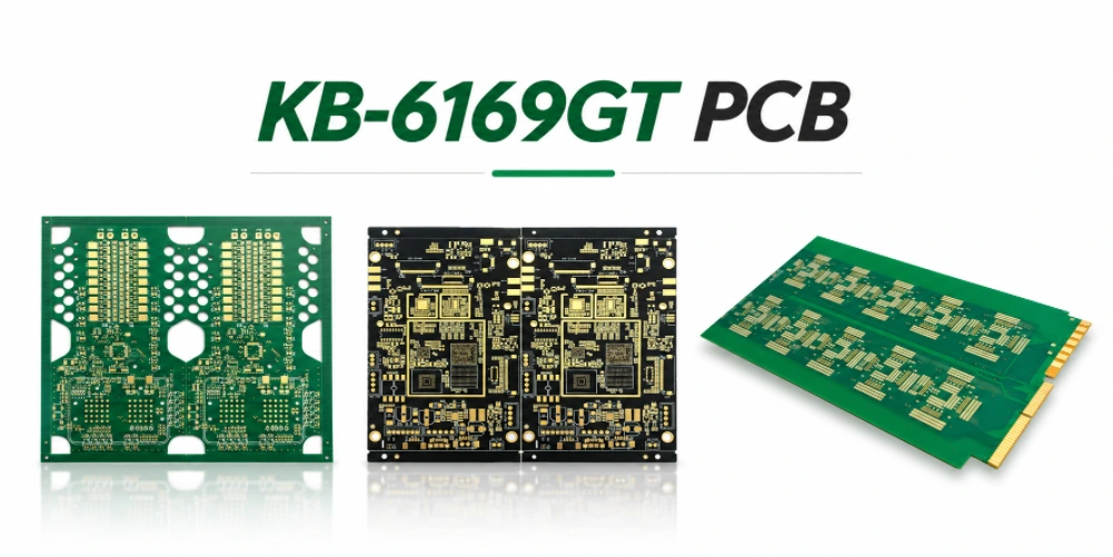
Fabrication et assemblage de circuits imprimés haute température de transition vitreuse (KB-6169GT)
HIGHLEAP ELECTRONICS / KB-6169GT / ASSEMBLAGE DE PCB HAUTE Tg...
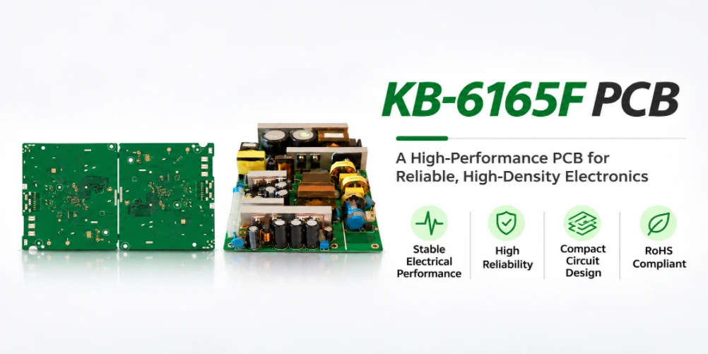
Fabrication et assemblage de circuits imprimés KB-6165F en Chine
HIGHLEAP ELECTRONICS / KB-6165F / FABRICATION ET...
Comment obtenir un devis pour les PCB
Nous réaliserons une analyse DFM/DFA pour vous et vous fournirons un rapport. Vous pouvez télécharger vos fichiers en toute sécurité via notre site web. Nous avons besoin des informations suivantes pour vous établir un devis :
-
- Gerber, ODB++ ou .pcb, spécifications.
- Liste de nomenclature si vous avez besoin d'un assemblage
- Quantité
- Temps de rotation
Outre la fabrication de circuits imprimés, nous proposons une gamme complète de services électroniques, incluant la conception de circuits imprimés, l'assemblage de cartes de circuits imprimés et des solutions clés en main. Que vous ayez besoin d'aide pour le prototypage, la vérification de la conception, l'approvisionnement en composants ou la production en série, nous vous offrons un accompagnement complet pour garantir la réussite de votre projet.
Pour les services PCBA, veuillez fournir votre nomenclature (BOM) et toute instruction d'assemblage spécifique. Nous proposons également des analyses DFM/DFA pour optimiser la fabricabilité et l'assemblage de vos conceptions, garantissant ainsi un processus de production fluide.