
Arlon 85NT PCB: Polyimide Fabrication and SMT Control
PCB manufacturing illustration; material grade and construction are confirmed in the project specification.
A high-temperature polyimide PCB laminate with nonwoven aramid reinforcement is used when thermal stability and low in-plane expansion are both important. Arlon 85NT is a 250°C Tg polyimide laminate and prepreg system reinforced with nonwoven aramid; its product information lists an X-Y CTE of approximately 6–9 ppm/°C. The finished board’s Z-axis behavior, plated-hole construction and moisture condition still require separate engineering control.
The material illustrates two different reliability paths. Aramid reinforcement restrains in-plane movement and can improve dimensional stability, while constrained constructions can still experience substantial through-thickness expansion and plated-barrel strain. Moisture absorbed by the polyimide and aramid also has to be managed between bare-board fabrication, storage and SMT reflow.
High-Temperature Polyimide PCB with Nonwoven Aramid Reinforcement
The material’s aramid reinforcement restrains movement along the board surface, helping align the substrate with certain low-expansion packages. Its high-Tg polyimide resin provides a different temperature response than standard epoxy. However, the reinforcement does not constrain the thickness direction to the same extent: Arlon lists approximately 2.3% Z-axis expansion from 50–260°C für das Material.
| Veröffentlichte Referenz | 85NT value | Meaning for a finished PCB |
|---|---|---|
| Resin / reinforcement | Polyimide / nonwoven aramid | Distinct cure, moisture and hole-processing behavior |
| Tg | 250°C, supplier data | Thermal property; not an assembly temperature limit |
| X-Y CTE | About 6–9 ppm/°C | Relevant to package/board expansion mismatch |
| Z-axis expansion (50–260°C) | 2.3% | Important input to plated-hole thermal fatigue assessment |
| Wasseraufnahme | About 0.6% in a defined supplier test | A reason to control handling and drying |
A simplified dimensional example shows why low X-Y CTE does not automatically mean low plated-hole strain. The plated-through-hole reliability of polyimide PCB fabrication depends on board thickness, Z-axis expansion, hole geometry and copper-barrel properties, not on in-plane expansion alone.
Das selection of polyimide PCB materials for low-CTE packages should begin with the dominant reliability requirement: package solder-joint strain, through-hole life, thermal endurance, dielectric behavior or a combination. 85NT is not automatically superior for every application simply because it is a polyimide.
Published Tg and X-Y CTE of High-Temperature Aramid Polyimide
Arlon describes 85NT as a 250°C Tg polyimide laminate and prepreg system reinforced with nonwoven aramid. Its product information gives low in-plane expansion in the approximate 6–9 ppm/°C range, while the processing guide discusses finished-board X-Y values and a substantially higher Z-axis expansion. Those directions must be kept separate: low X-Y CTE can help control package-to-board movement, but it does not mean the plated-hole barrel experiences low through-thickness strain.
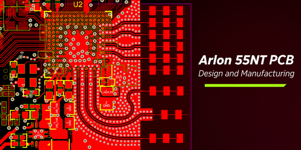
Polyimide PCB Lamination: Prepreg Moisture, Cure and Registration
85NT multilayers demand attention to resin advancement and the thermal mass of the lay-up. Arlon’s published processing recommendation uses a high-temperature cure stage around 218°C with a three-hour cure at temperature, supported by controlled heating, cooling and vacuum. These are material-supplier process starting conditions, not an interchangeable recipe for all press configurations.
Das polyimide PCB lamination process must be assessed for the actual layer count, copper pattern, press package and monitored product temperature. Incomplete cure can weaken interlaminar bonding, while uncontrolled heating gradients can cause nonuniform consolidation or registration shifts.
- Prepare the inner layers: inspect copper definition, adhesion treatment and layer orientation before any moisture-sensitive material is exposed.
- Condition the materials: follow the approved drying and prepreg handling instructions; minimize the interval between conditioning and lay-up.
- Execute the qualified cure: verify that the product—not only the press set point—reaches and maintains its required thermal profile.
- Messen Sie das Ergebnis: examine pressed dielectric thickness, layer registration and representative cross-sections before downstream drilling.
Nonwoven aramid can support dimensional stability, but copper distribution still affects the effective in-plane behavior. A documented multilayer PCB stack-up and copper-balance plan, supported by registration measurements, is more reliable than assumptions based on a bare laminate coupon.
A resin cure profile is not the same as a maximum material-temperature specification. Tg is a state-dependent property of the polymer after cure, whereas the press must give the resin enough time to reach that state. In a metal-heavy multilayer, the center of the book may lag the platen substantially. The thermal history required for full cure must therefore be evaluated at representative locations rather than inferred from a nominal press-program duration.
Vacuum Desiccation of 85NT Prepreg Before Multilayer Lamination
Arlon’s 85NT processing guide identifies moisture removal before multilayer lamination as a critical control. After the original vapor-barrier bag is opened, the supplier recommends vacuum desiccation for 8–12 hours at 29 inches of vacuum or greater as a starting condition. Inner layers and prepregs can also take up moisture during wet processing and handling, so the interval between drying and lay-up should be controlled and recorded. The production procedure must follow the current material documentation and the actual storage history.
PTH Reliability in Aramid-Reinforced Polyimide PCBs
Drilling 85NT is not identical to drilling a conventional woven-glass epoxy board. The organic aramid network changes cutting and fiber evacuation, while the polyimide resin requires a validated hole-wall preparation sequence. A hole can appear dimensionally acceptable yet retain smeared resin at an internal copper intersection, leading to inadequate metallurgical contact after copper deposition.
Mechanical Drilling of Aramid-Reinforced Polyimide PCBs
Das mechanical drilling of aramid-reinforced polyimide boards should be qualified against finished thickness, drill diameter, stack height, debris evacuation and wall roughness. Small drills need particular attention to blockage and tool wear.
Laser Microvia Formation in High-Density Polyimide PCBs
Where the construction requires laser-drilled microvias in high-density PCBs, ablation quality, dielectric residue and capture-pad cleanliness must be checked against the actual resin system and via geometry.
Desmear and copper deposition are connected operations. The copper plating process for reliable PTHs must provide a continuous deposit with adequate barrel and knee characteristics under the specified acceptance conditions.
| Fehlersymptom | Potential underlying mechanism | Nützliche Überprüfung |
|---|---|---|
| Intermittent through-hole open after cycling | Barrel fatigue or inner-layer separation | Thermal-stress coupon and cross-section |
| Copper skip / localized void | Residual smear or poor activation | Hole-wall and plating microsection |
| Rough drilled wall / fiber pull-out | Unsuitable drill or evacuation setting | Drilling trial and wall morphology |
| Layer breakout at a hole | Registration and drilling tolerance interaction | Drill-to-copper registration measurement |
A high-temperature polyimide does not remove the need for PCB microsection and thermal-stress inspection. Cross-sections, plated-hole measurements, continuity and job-specific thermal tests provide evidence about the finished interconnect rather than the raw material alone.
Where a small finished hole passes through many copper interfaces, registration and interconnect preparation are inseparable. Increasing desmear aggressiveness cannot correct a hole that is already outside the internal pad; increasing copper plating cannot create proper metal-to-metal contact through a persistent resin film. Process adjustments should target the actual defect mechanism identified in a microsection.
Z-Axis Expansion and Copper Ductility in Polyimide PTH Reliability
Arlon’s processing guide describes Z-axis CTE in the range of approximately 90–130 ppm/°C for constrained 85NT constructions and emphasizes the copper deposit’s elongation capability. Its guidance calls for plating with approximately 17–20% elongation at 45,000–50,000 psi tensile strength, and notes that 1.5 mil (0.038 mm) copper plating can improve plated-through-hole reliability. These are supplier process recommendations, not universal acceptance limits; the drawing, hole aspect ratio, coupon results and customer qualification plan govern the finished board.
POLYIMIDE PCB FABRICATION & SMT REVIEW
Taking an Arlon 85NT polyimide PCB into production?
Provide the approved material construction, stack-up, drill data and assembly requirements. Highleap can review the bare-board fabrication package and coordinate relevant moisture-handling, plated-through-hole inspection and SMT process information within the agreed project scope.
Include these details before fabrication review
- Exact 85NT laminate and prepreg designation, including storage history
- Finished board thickness, hole geometry, copper weights and plating requirements
- Moisture handling, bake instructions, reflow profile and inspection criteria
Moisture Baking Polyimide PCBs Before SMT Reflow
Polyimide resin and aramid reinforcement can absorb moisture during storage and wet fabrication steps. Rapid heating may convert trapped water into vapor and increase local pressure at interfaces. Blistering, delamination or internal separation can appear during solder mask cure, surface finishing, hot-air solder leveling, reflow or component rework.
Moisture control is therefore a chain of custody between bare-board fabrication and assembly—not a single bake performed early in production. Arlon publishes assembly guidance for 85NT that emphasizes drying and moisture-resistant packaging. The appropriate drying profile should be determined from the supplier document, the assembled-board restrictions and the intended processing sequence; it is not appropriate to prescribe one bake for every finished board.
| Übergabepunkt | Condition to control | Was ist zu dokumentieren? |
|---|---|---|
| Post-wet-processing fabrication | Residual water before subsequent heat exposure | Konditionierungs- und Lagergeschichte |
| Finished bare-board packaging | Humidity ingress and exposure time | Bag/seal condition and handling instructions |
| Before SMT reflow | Board moisture and oven profile | Approved bake if required; thermal recipe |
| After rework or further heat cycles | Cumulative thermal and handling exposure | Rework records and any required inspection |
Before soldering, moisture conditioning and the SMT reflow profile for moisture-sensitive PCBs must be coordinated with component and board thermal limits. After assembly, X-ray inspection of hidden BGA solder joints can identify certain joint defects, while continuity, cross-section and thermal testing address other failure modes.
Moisture management must also preserve solderability and product safety. A drying step that is appropriate for an unpopulated substrate may not be acceptable after temperature-sensitive components are mounted or after a finish has aged. Packaging instructions, maximum floor exposure and any required reconditioning should therefore be passed clearly between the PCB manufacturer and the assembly operation.
Moisture Bake for 85NT Boards Before SMT Reflow
Arlon’s assembly note reports that aramid reinforcement and polyimide resin can absorb moisture during exposure to humid conditions. It describes moisture levels in the approximate 0.1–0.9% range and a conventional drying approach of 110–150°C for 2–6 hours, depending on the board and its construction. This is supplier guidance, not a fixed recipe for every finished PCB. Copper cladding, board thickness, surface finish, storage time and component sensitivity must be considered, and any bake after component mounting requires separate approval.
85NT PCB Fabrication and Assembly Qualification
A material callout is incomplete if the procurement drawing does not identify the intended core and prepreg, copper construction, plated-hole criteria and material substitution rules. For 85NT, traceability of the specified reinforcement and resin system can matter to highly controlled programs, particularly when customers define a qualified material baseline. Changes should be evaluated under the applicable purchasing and design-approval procedure.
Bare-Board Qualification for High-Tg Polyimide PCB Fabrication
Das polyimide PCB fabrication and bare-board qualification package should include the approved stack-up, drill chart, copper weights, material callout, finished thickness and acceptance class.
SMT Assembly Documentation for Moisture-Sensitive Polyimide Boards
Das SMT assembly process for polyimide PCB products should be released with the BOM, placement data, assembly drawings, solder profiles and functional-test requirements.
Highleap Electronics can assess 85NT inquiries against the required fabrication and assembly scope, confirm whether the specified material form is available for the proposed construction, and identify inspection or qualification items needing agreement before production. The objective is a board whose material behavior, copper interconnects and assembly history are managed as one system.
Engineering conclusion. 85NT combines low in-plane expansion with high-temperature polyimide chemistry, but through-thickness expansion and moisture remain consequential. Successful application depends on qualified lamination, interconnect preparation and controlled handling all the way to SMT.
For programs requiring elevated reliability, a qualification plan should deliberately cover both SMT joints and copper-plated through-holes. A favorable X-Y CTE result is not evidence of barrel fatigue resistance, and an acceptable plated-hole microsection is not evidence of long-term BGA durability. Acceptance needs separate performance criteria for the mechanisms the application actually exposes.
Qualification Tests for 85NT Polyimide PCB and PCBA
A complete qualification plan should separate through-hole reliability from SMT package reliability. Bare-board evidence may include cross-sections, plated-hole measurements, continuity and thermal-stress coupons. Assembly evidence may include the approved moisture-conditioning record, reflow profile, inspection and functional test. A material’s 250°C Tg or low X-Y CTE is not a substitute for these board- and assembly-level results.
Arlon 85NT PCB or PCBA inquiry: Share the approved material designation, stack-up, drill information, assembly data and any qualification plan with Highleap Electronics using the PCB/PCBA quote form.

Über den Autor
Helen Chong
PCB-Lösungsberater & Manager für internationale Geschäftsentwicklung bei Highleap Electronics
Helen unterstützt internationale Entwicklungsteams mit umfassenden Lösungen für die Leiterplattenfertigung und -bestückung und begleitet Projekte von der schnellen Prototypenentwicklung bis zur stabilen Serienproduktion. Ihre Expertise umfasst Hochfrequenz- und HF-Leiterplatten, komplexe Multilayer-Aufbauten sowie starr-flexible und flexible Leiterplattentechnologien in verschiedenen Branchen.
Durch die Übersetzung technischer Anforderungen in praktische Fertigungspläne hilft sie Kunden dabei, die Herstellbarkeit zu verbessern, Risiken zu reduzieren und Kosten und Lieferzeiten zu optimieren – und gleichzeitig eine gleichbleibende Qualität in großem Umfang zu gewährleisten.

Empfohlen Beiträge
Arlon 86HP HDI Leiterplattenfertigung
Illustration zur Leiterplattenfertigung. Bestätigen Sie die Angaben...
KB-6169GT High-Tg Leiterplattenfertigung & -bestückung
HIGHLEAP ELECTRONICS / KB-6169GT / HIGH-Tg PCB BUILDSHave...
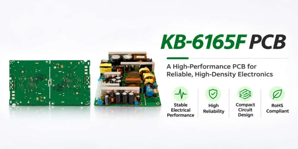
KB-6165F Leiterplattenfertigung und -bestückung in China
HIGHLEAP ELECTRONICS / KB-6165F / PCB-HERSTELLUNG &...
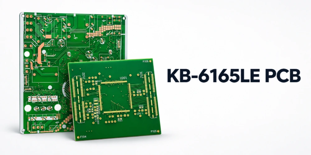
KB-6165LE Mehrlagige Leiterplattenfertigung und -bestückung
HIGHLEAP ELECTRONICS / KB-6165LE / MEHRLAGE-LEITERPLATTE...
So erhalten Sie ein Angebot für Leiterplatten
Wir führen eine DFM/DFA-Analyse für Sie durch und senden Ihnen anschließend einen Bericht zu. Sie können Ihre Dateien sicher über unsere Website hochladen. Für ein Angebot benötigen wir folgende Informationen:
-
- Gerber, ODB++ oder .pcb, Spezifikation.
- Stückliste, wenn Sie eine Montage benötigen
- Die Menge
- Wendezeit
Neben der Leiterplattenfertigung bieten wir umfassende Elektronikdienstleistungen an, darunter Leiterplattendesign, PCBA und schlüsselfertige Lösungen. Ob Sie Unterstützung beim Prototyping, der Designverifizierung, der Komponentenbeschaffung oder der Massenproduktion benötigen – wir bieten Ihnen umfassende Unterstützung für den Erfolg Ihres Projekts.
Für PCBA-Dienstleistungen geben Sie bitte Ihre Stückliste (BOM) und alle spezifischen Montageanweisungen an. Wir bieten auch DFM/DFA-Analysen an, um Ihre Designs hinsichtlich Herstellbarkeit und Montage zu optimieren und so einen reibungslosen Produktionsprozess zu gewährleisten.