
IT-601G PCB Manufacturing for Multilayer and HDI Boards
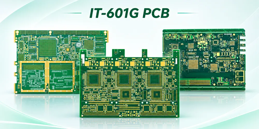
Illustration of dense PCB routing for an HDI build.
ITEQ IT-601G is a halogen-free, high-Tg material system for advanced HDI PCBs that need low through-thickness expansion and lower dielectric loss. The grade-specific datasheet reports 1.1% Z-axis expansion from 50°C to 260°C. It also reports a 230°C Tg by DMA and a 210°C Tg by TMA. For stacked microvias, the release decision still depends on the construction and on evidence from the actual interconnect sequence.
Resolve conflicting IT-601G values before simulation
Online material summaries can show 10 GHz Dk and Df as 3.5 and 0.0060 at 50% resin content, or label 230°C as a TMA result. For the model and purchase specification, record the grade, document number, revision, resin content, frequency and method together. The ITEQ IT-601G grade sheet W-CTE-1002-64D, Rev. 1.0-26 describes the following specimen results. Do not reconcile differing sources by averaging their values or by moving Dk and Df from one row to another.
| Eigenschaft | Gemeldetes Ergebnis | Method or construction |
|---|---|---|
| Dk / Df bei 1 GHz | 3.5 / 0.0055 | 70 % Harzanteil; IPC-TM-650 2.5.5.9 |
| Dk / Df bei 10 GHz | 3.28 / 0.0064 | 70 % Harzanteil; IPC-TM-650 2.5.5.13 |
| Tg | 230°C DMA; 210°C TMA | IPC-TM-650 2.4.24.4 and 2.4.24, respectively |
| Z-Achsen-Erweiterung | 1.1 % von 50 °C bis 260 °C | IPC-TM-650 2.4.24; Laminatprobe |
| Td / T260 / T288 | 420°C / >60 min / >60 min | Td at 5% mass loss; T-times measured separately |
Arbeiten jederzeit weiterbearbeiten können. Jede Präsentation und jeder KI-Avatar, den Sie von Grund auf neu erstellen oder hochladen, IT-601GTC und IT-601GBS to identify the copper-clad laminate and prepreg in the material record. For an impedance or loss model, ask for construction-specific inputs for the actual glass style, pressed dielectric and copper foil. Keep the model and coupon on that same revision. A 70% resin-content datasheet value can be valid and still be the wrong input for a layer with a different construction.
Plan evidence before each lamination hides an interface
IT-601G’s reported Z-axis expansion is useful for screening where temperature excursions load the vertical interconnects. In a stacked via column, however, each copper connection depends on its own geometry, target preparation and plating. A low-expansion laminate does not prevent a weak interface from opening. A staggered transition trades routing area for the ability to avoid placing the next via directly on the previous filled via. Check whether the package can escape with that arrangement before committing to a stacked column.
Hypothetical 2+N+2 process review. In this example two build-up layers are added symmetrically on either side of a central multilayer structure. Some signals pass through a buried via in the center, then through two laser microvias on one side. The checkpoints below describe what to agree for this example; they are neither a claim about a Highleap production line nor a universal process traveler.
| Build-Phase | Risk to close | Evidence to define with the fabricator |
|---|---|---|
| Central subassembly | Buried-hole barrel or land defects become hard to isolate after build-up. | Register the inner layers and define representative checks of buried span, plating and any required fill before it is covered. |
| First build-up pair | Poor contact to the target, incomplete fill or a recessed fill surface under the next via. | Agree on local pressed thickness, pad capture, fill profile and planarity inspection at sites that represent the next landing. |
| Second build-up pair | Misregistration or weak copper interfaces within the stacked path. | Section representative stack geometry and define a continuity coupon with each interface included in the measured path. |
| Qualification and release | Intermittent opens during temperature excursions; integration errors at fine-pitch lands. | Agree on thermal exposure and resistance monitoring, board net test, and finished land/assembly inspection as distinct requirements. |
An electrical coupon that bypasses the longest or most demanding stack answers the wrong question. Retain the panel or coupon identity through stress and sectioning so failed locations can be compared to geometry. A section at ambient temperature can look acceptable at the sampled plane even when an interface opens only while hot. For sequentielle Laminierung, decide which observations need to occur during fabrication and which can be made on the completed structure. The IPC-TM-650 method index provides test references; use the method, conditioning and limits specified for the actual program.
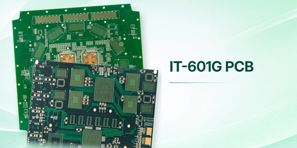
HDI PCB illustration. Artwork does not establish the buried interconnect construction or reliability.
Put copper foil changes under revision control
The ITEQ sheet lists 18 µm RTF and RTF2 low-profile foils and 18 µm HTE standard-profile foil with separate peel-strength results. Those are not roughness specifications. Two foil constructions at the same thickness can differ in adhesion treatment and conductor loss. For loss-sensitive layers, specify the permitted foil and the surface information required by the model. Keep the test coupon on the same layer construction as the routed traces.
A foil or prepreg substitution can change more than one result. The new bonding package can change the final dielectric spacing and laser depth, while a new foil treatment can change electrical loss without a large change in TDR impedance. Record proposed substitutions against four items: the pressed thickness, landing and fill geometry, impedance and loss inputs, and the qualification evidence. If any has changed, identify which requirement needs to be demonstrated again. This connects Impedanzkontrolle with the process route instead of treating the two as independent drawing approvals.
Leiterplattenfertigung und -montage
Planning an IT-601G PCB build?
Highleap kann die Anforderungen an die Platinenkonstruktion und -montage gemeinsam überprüfen.
Include the via map, lamination sequence and the qualification requirements for buried interfaces.
Release the HDI stack and the assembly together
Memory, SiP and other compact devices can force via-in-pad and place limits on board and package coplanarity. Agree on pad finish and solder-mask registration, and verify that the released drawings address via fill, cap and flatness where solder joints sit above vias. Include panel handling in the assembly review. X-ray can aid hidden solder-joint inspection; bare-board coupons and sections remain necessary when the acceptance plan requires evidence of buried interconnect integrity.
Für ein IT-601G fabrication and PCBA estimate, provide the controlled material revision, core and prepreg constructions, via span and stack maps, foil and electrical inputs, and coupon acceptance requirements. Pair those files with the package footprints, BOM, placement file and assembly drawing. Highleap Electronics can then review material sourcing, the build-up sequence, and the first-article inspection scope against one release package.

Über den Autor
Charles L.
PCB-CAM- und Fertigungsingenieur bei Highleap Electronics
Charles verfügt über mehr als zehn Jahre Erfahrung in der Leiterplatten-CAM-Entwicklung und Elektronikfertigung. Seine Spezialgebiete sind die Verifizierung von Leiterplattendateien, DFM-Analysen und die Produktionsvorbereitung für Multilayer-, HDI-, HF- und Hochgeschwindigkeitsleiterplatten. Dank seiner Expertise in Genesis, InCAM und CAM350 gewährleistet er präzise Daten, stabile Prozesse und eine hohe Fertigungsausbeute.
Bei Highleap Electronics konzentriert er sich auf Prozessoptimierung und die Bewertung der Herstellbarkeit, um Kunden dabei zu helfen, Risiken zu reduzieren, Lieferzeiten zu verkürzen und zuverlässige Produktionsergebnisse zu erzielen.

Empfohlen Beiträge
Aufbau von IT-602G HDI-Platinen für SSDs und Speichermodule
IT-602G Leiterplattenbeispiele für HDI, SSD und Speichermodule...
IT-988GL Backplane-Leiterplatten mit Low-CTE-Prozesskontrolle
IT-988GL Mehrlagen-Leiterplattenfertigung...
Arlon 85NT Leiterplatte: Polyimid-Fertigung und SMT-Steuerung
Illustration zur Leiterplattenherstellung; Materialgüte und...
Hochwertige Arlon 33N Leiterplattenfertigung
Illustration zur Leiterplattenfertigung. Bestätigen Sie die Angaben...
So erhalten Sie ein Angebot für Leiterplatten
Wir führen eine DFM/DFA-Analyse für Sie durch und senden Ihnen anschließend einen Bericht zu. Sie können Ihre Dateien sicher über unsere Website hochladen. Für ein Angebot benötigen wir folgende Informationen:
-
- Gerber, ODB++ oder .pcb, Spezifikation.
- Stückliste, wenn Sie eine Montage benötigen
- Die Menge
- Wendezeit
Neben der Leiterplattenfertigung bieten wir umfassende Elektronikdienstleistungen an, darunter Leiterplattendesign, PCBA und schlüsselfertige Lösungen. Ob Sie Unterstützung beim Prototyping, der Designverifizierung, der Komponentenbeschaffung oder der Massenproduktion benötigen – wir bieten Ihnen umfassende Unterstützung für den Erfolg Ihres Projekts.
Für PCBA-Dienstleistungen geben Sie bitte Ihre Stückliste (BOM) und alle spezifischen Montageanweisungen an. Wir bieten auch DFM/DFA-Analysen an, um Ihre Designs hinsichtlich Herstellbarkeit und Montage zu optimieren und so einen reibungslosen Produktionsprozess zu gewährleisten.