BGA Packages
Unlock Efficiency and Cost Savings with Highleap’s BGA Packages: Streamlined Manufacturing, Reduced Production Costs.
What is BGA ?
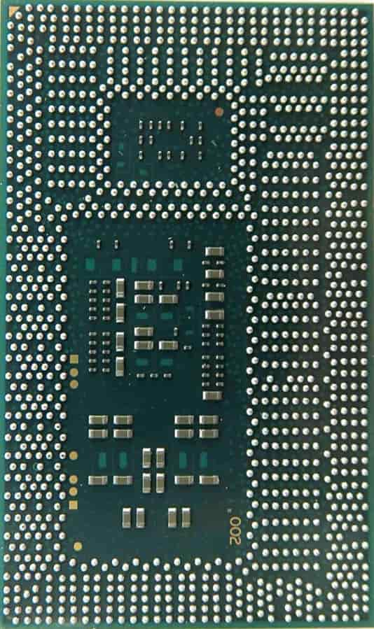
PCB BGA, or Printed Circuit Board Ball Grid Array, is a specialized form of surface-mount packaging designed exclusively for integrated circuits (ICs). In contrast to traditional packaging methods like the Quad Flat Pack (QFP), which rely on side connections, BGA takes a unique approach to establish connections, primarily for permanent device mounting.
Traditional packages like QFP face limitations due to their sides, requiring closely spaced and relatively small pins to achieve necessary connectivity. In contrast, BGA, short for Ball Grid Array, utilizes the package’s underside, offering ample space for connections and enabling full utilization of the bottom surface.
Within a BGA package, pins are arranged in a grid pattern, hence the name “Ball Grid Array.” These pins work alongside strategically positioned solder balls on the package’s bottom surface, ensuring robust electrical connections. This connection mechanism is facilitated by a corresponding set of copper pads integrated onto the BGA printed circuit board, enabling reliable and efficient connections between integrated circuits and the PCB.
PCB BGAs find extensive use across diverse electronic devices and applications, especially in scenarios demanding compact dimensions, a high number of pins, and effective thermal management. Companies like Highleap, a reputable PCB & PCBA manufacturer, play a vital role in producing high-quality BGA components that drive innovation in the electronics industry.
Highleap BGA – PCB Prototype the Easy Way
Commonly Used BGA Package Types?
BGA (Ball Grid Array) is a popular package type used in integrated circuits (ICs) and electronic components. It provides a compact and reliable method for mounting ICs onto printed circuit boards (PCBs). Here are some commonly used BGA package types:
PBGA
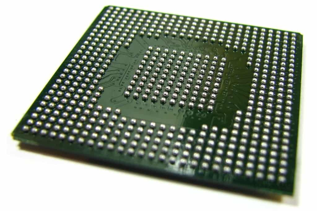
PBGA (Plastic Ball Grid Array) is a widely used BGA package type. It features a plastic substrate with a grid array of solder balls on the bottom, which connects the IC to the PCB. PBGA packages offer good thermal and electrical performance and are available in various sizes and ball counts.
CBGA
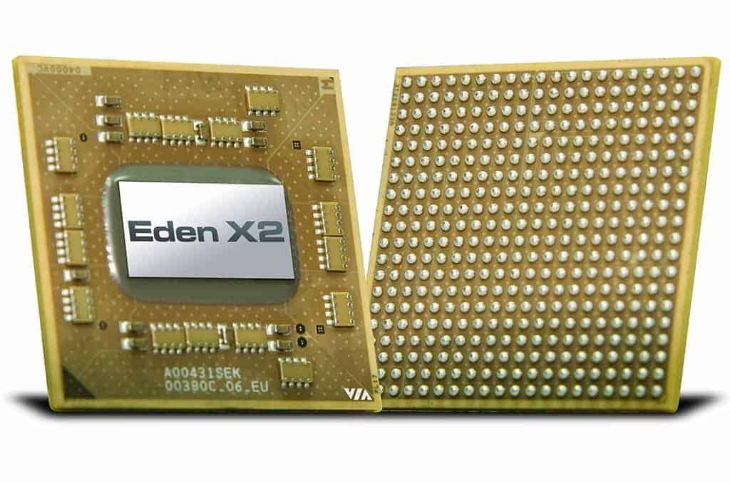
CBGA (Ceramic Ball Grid Array) packages use a ceramic substrate instead of plastic. Ceramic offers better thermal conductivity and stability compared to plastic, making CBGA suitable for high-performance applications requiring efficient heat dissipation. CBGAs are commonly used in processors, graphics chips, and other high-power ICs.
TBGA
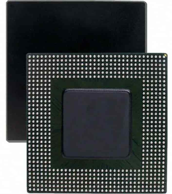
TBGA (Thin Ball Grid Array) packages are designed to have a thinner profile compared to traditional BGA packages. They are used in applications where space is limited, such as laptops, tablets, and mobile devices. TBGA packages typically have a smaller ball pitch and a reduced thickness to meet the size constraints.
FBGA
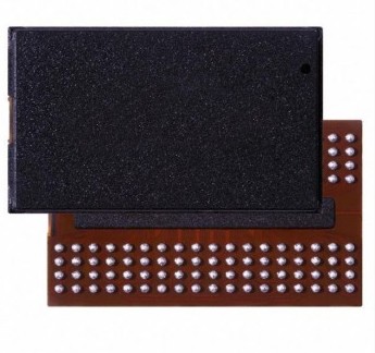
FBGA (Fine Ball Grid Array) packages have a smaller ball pitch compared to standard BGA packages. They are used in applications that require higher pin densities and improved electrical performance. FBGAs are commonly found in memory modules, such as DDR3 and DDR4 modules.
uBGA
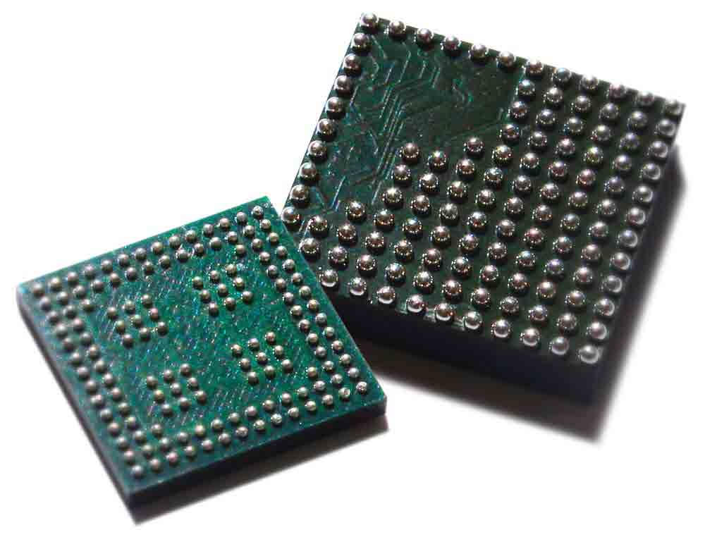
uBGA (Micro Ball Grid Array) packages are miniaturized versions of BGA packages, designed for extremely small form factors and high pin densities. They are used in compact electronic devices like smartphones, wearables, and IoT devices. uBGAs have very small ball pitches and are challenging to assemble and rework due to their size.
CCGA
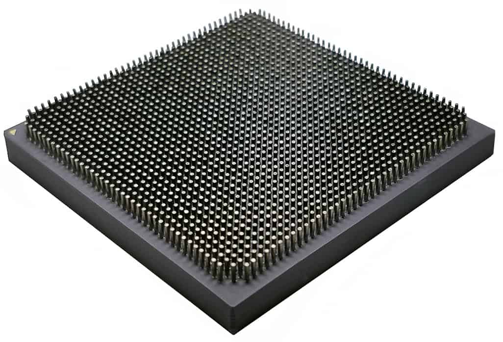
CCGA (Ceramic Column Grid Array) packages feature ceramic columns instead of solder balls for electrical connections. The ceramic columns provide better reliability and mechanical strength, making CCGAs suitable for applications with high shock and vibration requirements, such as automotive and aerospace electronics.
These are just a few examples of commonly used BGA package types. The specific package type chosen for a particular application depends on factors such as size constraints, thermal requirements, pin count, electrical performance, and cost considerations.
Advantages of BGA Package
In the realm of electronics, BGA packages offer space efficiency, thermal prowess, stable electrical performance, and streamlined manufacturing, reducing costs. Highleap, a leading PCB & PCBA manufacturer, harnesses BGA’s advantages for top-quality, cost-effective solutions.Advantages of BGA Package are as follows:
Efficient PCB Space Utilization
BGA packages offer efficient utilization of PCB space. With fewer components involved and a smaller footprint, they help save space on custom PCBs, greatly enhancing PCB space efficiency. This is especially valuable in compact electronic devices.
Enhanced Thermal Performance
BGA packages excel in thermal management. When the silicon chip is mounted on top, most of the heat can efficiently transfer downward through the ball grid array. Conversely, when the silicon chip is mounted on the bottom, the backside of the die is connected to the top of the package, enabling effective cooling. This thermal efficiency reduces the risk of overheating and enhances the reliability of electronic components.
Improved Electrical Performance
BGA packages provide stable electrical performance on a large scale. They lack bendable or breakable pins, reducing the risk of electrical connectivity issues. This stability ensures consistent and reliable performance of integrated circuits.
Streamlined Soldering Process
BGA packages typically feature relatively large solder balls. This makes large-area soldering more manageable and convenient during the manufacturing process. As a result, PCB production speed increases, and the overall production yield is improved. Additionally, the larger solder balls make rework, if needed, more straightforward.
Minimized Lead Damage
BGA leads consist of solid solder balls, which are less prone to damage during handling, assembly, or use compared to traditional packages with fragile leads. This durability contributes to the longevity and robustness of electronic devices.
In achieving these advantages, partnering with experienced PCB and PCBA manufacturers is crucial. Highleap, a reputable PCB & PCBA manufacturer, stands as a reliable partner in realizing the benefits of BGA packages. Our expertise in manufacturing and assembly processes ensures high-quality and cost-effective solutions for a wide range of electronic applications.
Factors Affecting PCB BGA Assembly Quality?
The quality of PCB BGA (Ball Grid Array) assembly can be influenced by various factors. Ensuring proper attention to these factors is crucial to achieving reliable and high-quality BGA assemblies.With Highleap’s dedication to these factors and the implementation of stringent manufacturing processes, we consistently deliver high-quality and reliable BGA assemblies. Our collaborative approach, involving PCB designers, assembly technicians, and quality control personnel, ensures the effective management of these factors, resulting in successful BGA assembly for a diverse range of applications. Here are some key factors that can impact PCB BGA assembly quality:
1
Solder Paste Application
The application of solder paste is critical for achieving good solder joints. Factors such as the stencil design, solder paste composition, and printing process parameters (e.g., squeegee pressure, speed, and alignment) can affect the solder paste deposition. Proper solder paste application ensures an adequate amount of solder for forming reliable connections.
2
BGA Component Alignment:
Accurate alignment of the BGA component on the PCB is crucial. Misalignment can result in poor solder connections or shorts between adjacent solder balls. Adequate inspection and control during the placement process help ensure the correct positioning of the BGA component on the PCB.
3
Solder Reflow Profile
The solder reflow process involves heating the PCB to melt the solder paste and form the solder connections. The reflow profile includes parameters such as preheat, soak, and peak temperatures, as well as the ramp-up and ramp-down rates. A well-optimized reflow profile ensures proper wetting and reflow of the solder paste, avoiding issues like insufficient solder volume, voids, or solder ball collapse.
4
Thermal Considerations
BGA packages can generate significant heat during operation. Thermal management is crucial to prevent excessive heat buildup, which can affect the reliability of the solder joints. Proper thermal design, including the use of thermal vias, heat sinks, and adequate PCB copper traces, helps dissipate heat effectively and prevents thermally-induced failures.
5
PCB Design Considerations
The PCB design plays a vital role in BGA assembly quality. Design factors such as pad layout, via placement, and solder mask design affect the solder joint formation and reliability. Proper pad size, shape, and spacing are important to ensure sufficient solder wetting and prevent solder bridging or solder ball misalignment.
6
PCB Material Selection
The choice of PCB materials can impact BGA assembly quality. Factors such as the coefficient of thermal expansion (CTE) of the PCB material should be compatible with the BGA component and the assembly process. Mismatched CTEs can lead to thermal stress and solder joint failures over time.
7
Inspection and Testing
Thorough inspection and testing processes are essential for ensuring the quality of BGA assemblies. Techniques such as X-ray inspection, automated optical inspection (AOI), and electrical testing help detect defects like insufficient solder volume, misalignment, shorts, or open connections. Proper inspection and testing procedures help identify and rectify any issues before the final product is deployed.
Highleap BGA Capability
The regular production capacity of BGA in our factory is as follows. If you have special requirements, please contact us at Highleap. We have a professional technical process team:
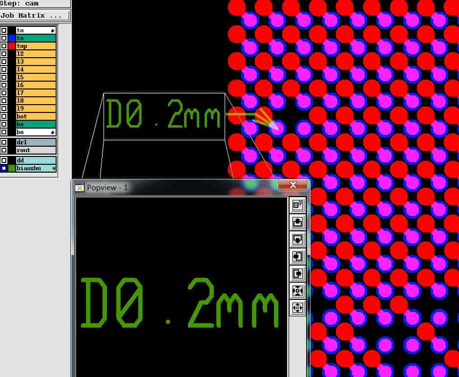
The minimum diameter of BGA pad is 0.2MM (the sample limit can be 0.15MM).
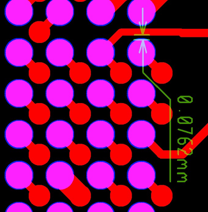
The minimum BGA to line is 3MIL (the prototype limit can be 2.5MIL).
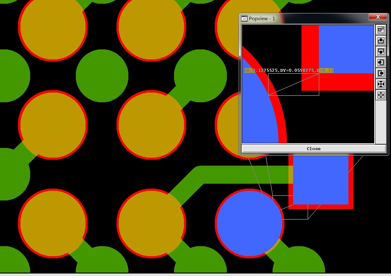
The minimum distance from the BGA solder pad edge to solder pads edge of other components is 0.15mm

The minimum distance from the center of one BGA solder pad to the center of another BGA solder padis 0.35mm.
