Heavy Copper PCB
Highleap committed to delivering the highest quality heavy copper PCBs that meet even the most demanding specifications and reliability needs.
What’s Heavy Copper PCB
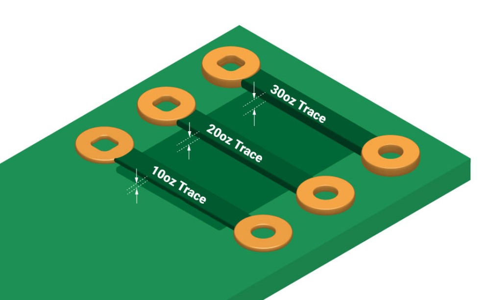
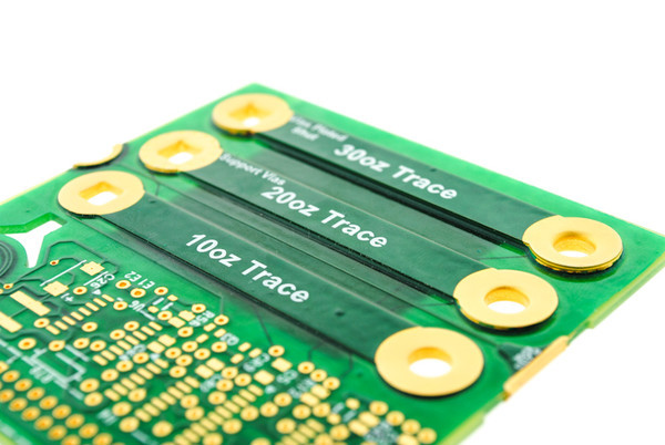
Heavy copper PCB refers to a type of printed circuit board (PCB) that has a thicker copper layer than standard PCBs. Typically, a standard PCB will have a copper thickness of 1oz (35 µm) or 2oz (70 µm), while a heavy copper PCB will have copper thicknesses of 3oz (105 µm) or more.
The increased copper thickness allows for higher current-carrying capacity, better thermal management, and improved mechanical strength of the PCB. Heavy copper PCBs are commonly used in high-power applications such as power supplies, automotive electronics, industrial control systems, and aerospace and defense systems.
Manufacturing heavy copper PCBs involves a specialized process that includes multiple plating and etching steps to achieve the desired copper thickness. The process requires advanced equipment and expertise, which can result in higher production costs compared to standard PCBs. However, the benefits of using heavy copper PCBs in high-power applications make them a cost-effective solution in the long run.
The Benefits of Heavy Copper PCB
The main benefits of thick copper PCBs are the ability to handle higher power, dissipate heat more effectively, improve high-speed signal performance, and provide greater mechanical robustness. These advantages come at the cost of higher material and manufacturing costs compared to standard copper PCBs. Specific advantages of thick copper PCBs include:
Higher current carrying capacity
The thicker copper traces and planes can carry higher currents thanks to their lower resistance. This makes heavy copper PCBs suitable for high power applications.
Lower impedance
Heavy copper PCBs have lower impedance which is desirable for high-speed signals and high frequency circuits.
Better heat dissipation
The extra copper acts as a better heat sink, allowing heat from components to dissipate more efficiently. This is important for applications with high power requirements.
Increased mechanical strength
The thicker copper layers provide more rigidity, making the PCB less prone to flexing, twisting and vibration. This is useful for applications that experience mechanical stress.
Lower voltage drop
Since the thicker copper traces have lower resistance, there is a lower voltage drop across them for a given current. This ensures a more stable supply voltage.
Better signal integrity
The lower impedance and resistance of heavy copper traces can help improve signal rise times, overshoot and ringing, leading to better signal integrity.
Reduced EMI and noise
The thicker copper planes provide better shielding which can help reduce electromagnetic interference and noise on the PCB.
Standard PCB VS Thick / Heavy Copper PCB
- Copper thickness: Standard PCBs typically use 1oz or 2oz copper layers while thick copper PCBs use 4oz to 20oz copper. The thicker copper provides benefits like higher current carrying capacity and lower impedance.
- Cost: Thick copper PCBs cost more due to the extra cost of the thicker copper laminate and the higher complexity of the manufacturing process.
- Manufacturing process: The thicker copper requires adjustments to the fabrication process like using stronger etchants, larger drill bits, and thicker solder mask. Standard PCB manufacturing equipment and chemicals may not work well for thick copper boards.
- Current carrying capacity: Thick copper PCBs can carry significantly higher currents due to the lower resistance of the thicker copper traces and planes. Standard PCBs are limited to lower power applications.
- Heat dissipation: The thicker copper layers in heavy copper PCBs allow for better heat spreading and dissipation from components, making them suitable for high power applications. Standard PCBs have poorer thermal performance.
- Mechanical strength: The extra copper provides thick copper PCBs with greater rigidity and durability, making them less prone to flexing and warping. Standard PCBs are more flexible.
- Impedance: Thick copper PCBs have lower impedance traces which is desirable for high speed digital signals and RF/high frequency circuits. Standard PCBs have higher impedance.
So in summary, the main differences come down to materials, manufacturing, cost, power handling capability, thermal performance, mechanical strength and impedance characteristics. Thick copper PCBs provide benefits for applications requiring high power, heat dissipation and signal integrity – at a higher price point.
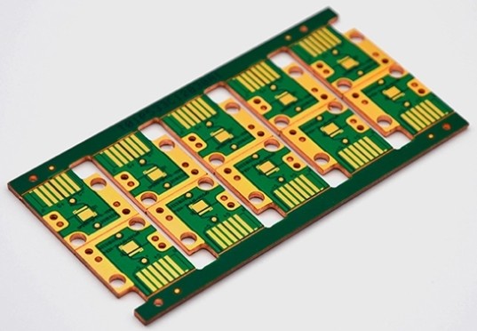
Heavy Copper PCB Design Guidelines
For heavy copper PCB design you’ll need wider traces, larger vias, thicker soldermask to account for the increased copper weight. Designing heavy copper PCBs can be more complex than designing standard PCBs.
Heavy/Thicker copper
Increased copper weights when needed – Only opt for 4oz, 6oz or heavier copper if it offers benefits like higher current capacity or lower impedance.
Use larger diameter vias
Thicker vias are needed to drill through the increased copper thickness. Start with 0.6mm vias for 4oz copper and go up to 0.8mm for thicker copper.
Increase trace widths
Since thick copper has lower resistance, wider trace widths can be used. Start with 0.2-0.3mm traces for 4oz-6oz copper and up to 0.5mm for thicker copper.
Increase annular ring sizes
Increase annular ring size is good for heavy copper PCB. Annular rings of 0.25mm or more can help prevent drill bit damage. The heavy copper requires more drilling force.
Guidelines for Heavy PCB Production
The process begins with the design of the PCB. Using a CAD (Computer Aided Design) program, engineers design the circuitry to be used. The design will specify the layers of the board and the placement of components, including where the heavy copper will be.
Material Cutting
The base material (usually a type of fiberglass like FR4) is prepared. Depending on the design, it may be pre-coated with a thin layer of copper.
Drilling
After etching, holes are drilled into the board for component leads. The location, size, and quantity of these holes are determined by the PCB design.
Plating
The drilled holes (vias) are then plated with copper to create a solid connection between the layers of the board.
Outer dry film
A layer of photoresist is applied to the board, then the circuit pattern is printed onto the photoresist using a special type of light. Where the light hits, the photoresist hardens. This hardening creates a protective barrier over the areas where the copper should remain.
Copper Deposition
Heavy copper PCBs undergo electroplating, where copper is added by immersing the board in a copper sulfate solution and passing an electric current through it. Copper ions adhere to specific areas, and thickness is adjusted by varying the process duration. Heavy copper PCBs generally range from 3oz (105μm) to 10oz (350μm) but can exceed 20oz (700μm) for extreme copper PCBs.
Etching
The board is then submerged in a chemical bath that etches away the unprotected copper. The hardened photoresist protects the copper that forms the circuitry from being etched away.
Solder mask
A solder mask is applied to the board. This layer helps to insulate the copper tracks from accidental contact with other metal, solder, or conductive bits. It also protects the copper from corrosion.
Silkscreen printing
The component designators and other markings are then printed onto the solder mask.
Testing
The finished board is thoroughly tested for functionality. This includes electrical tests to ensure there are no shorts or breaks in the circuitry, and sometimes additional tests depending on the intended application of the PCB.
Application of thick copper PCB
Heavy copper PCBs play a vital role in various industries and applications that demand high current carrying capacity, excellent heat dissipation, and robustness in challenging operating conditions. Here are some key applications of heavy copper PCB.
Power Electronics
Heavy copper PCBs are extensively used in power electronics applications, such as power supplies, inverters, motor drives, and electric vehicle (EV) chargers. The increased copper thickness helps to handle high currents without significant voltage drops or excessive heating. These PCBs can efficiently carry and distribute power, ensuring optimal performance and reliability.
Heat Dissipation
Heavy copper PCBs have excellent thermal conductivity, allowing for efficient heat dissipation. This property makes them suitable for applications with high-power components that generate significant heat, such as power amplifiers and power modules. The heavy copper layers act as heat sinks, reducing the operating temperature of critical components and enhancing overall system reliability.
RF and Microwave Applications
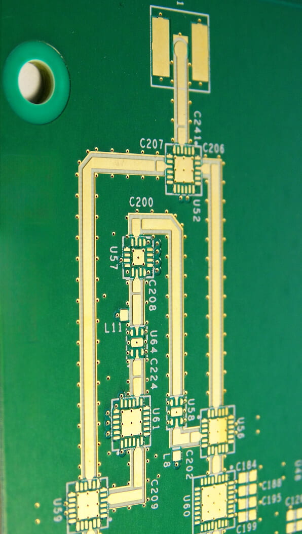
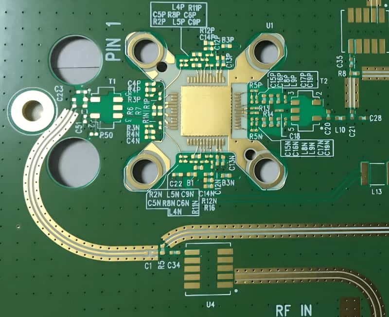
Heavy copper PCBs find applications in RF and microwave circuits due to their low impedance characteristics. They are used in HF devices, antennas, RF amplifiers, radar systems, and telecommunication equipment. The increased copper thickness reduces signal losses and improves signal integrity, making them suitable for high-frequency applications.
High Current Applications
Heavy copper PCBs are ideal for circuits that require high current handling. Industries like aerospace, automotive, industrial equipment, and renewable energy systems often utilize heavy copper PCBs in applications like power distribution, bus bars, and energy storage systems. The heavy copper layers provide low impedance paths, minimizing resistive losses and voltage drops.
Automotive Electronics
The automotive industry extensively utilizes heavy copper PCBs in various electronic systems, including engine control units (ECUs), lighting systems, electric power steering, battery management systems (BMS), and safety systems. These PCBs can handle high currents generated by automotive power systems and provide reliable connections even under harsh operating conditions.
Harsh Environment
Heavy copper PCBs offer enhanced mechanical strength and durability, making them well-suited for harsh environmental conditions. They are resistant to thermal cycling, vibration, and mechanical stress, making them suitable for aerospace, defense, and industrial applications where reliability and ruggedness are crucial.
Suggestion for Heavy Copper PCB design
Please contact Highleap Team for details.
Understand the Fabrication Process
The manufacturing process for thick copper PCBs involves several steps, including drilling, pattern plating, and etching. Each of these steps can affect the quality of the finished PCB, and it’s important to understand how they work and to specify your requirements accurately to Highleap Team.
Thermal Management
Thick copper PCBs are often used in applications that generate a significant amount of heat. The high thermal conductivity of copper can help to dissipate this heat, reducing the risk of thermal stress and failure. When designing your PCB, consider how the heat will be generated and distributed, and how the thick copper can help to manage this.
Mechanical Stability
Thick copper can add significant weight to a PCB, which can cause mechanical stress and potentially lead to failure. To mitigate this, you can consider using a thicker substrate, or adding additional support structures to the board.For example, standard FR4 might not be sufficient, and you might need to use materials like polyimide for better thermal stability.
Signal Integrity
Thick copper can cause signal integrity issues, particularly in high-speed digital or high-frequency analog circuits. It is vital to consider factors like impedance matching, crosstalk, and signal attenuation when designing these circuits.
Design for Manufacturability (DFM)
DFM is a crucial aspect to consider when designing any PCB, including thick copper ones. Ensure that your design follows good practice rules like maintaining minimum trace widths, adequate space between traces, and having robust via designs.
Layout & Layer Stackup
Due to the increased thickness, you may need to adjust your layout techniques. The thicker traces could necessitate broader spacing and may also require altered power and ground plane setups. For stack up, ensure that your layer stackup is designed correctly to maintain impedance control. More layers might be needed to meet the power requirements.
Highleap’s capabilities in thick copper PCBs
Highleap has industry-leading technology and facilities. We provide high-density solutions, compact form factors, design flexibility, and fast turnaround. Contact us now, and our Heavy Copper PCB experts will create a customized solution that meets your size, performance, and budget requirements.
When using heavy copper PCBs in certain applications, it is important to consider their performance.
According to their requirements, the heavy copper PCB should have the following features:
- A minimum board size of 6mm by 6mm and a maximum board size of 457mm by 610mm.
- Copper thickness is greater than 3oz for each square foot.
- Solder mask color should be either green, blue, red, black, white, purple and so on.
- Silkscreen color is white, yellow, or black and so on.
- A board thickness between 0.6mm and 6mm.
- Maximum external layer copper weight should be 15oz.
- The surface finishing should be Immersion Gold, OSP, HASL and so on.
- The finished thickness is between 0.020 — 0.275 inches.
