
Networking&Communication PCB
Highleap a complete integrated solution from design and engineering support, to production and full system assembly.
What is Communication PCB
In the field of communications, communication PCB boards play a crucial role in various applications such as wireless networks, transmission networks, data communications, and fixed-line broadband. These PCB boards encompass a range of products including backplanes, high-speed multilayer boards, high-frequency microwave boards, HDI boards and multi-function metal substrates.
PCB requirements in the communications field are divided into subdivisions such as communication devices and mobile terminals. Communication equipment is mainly used for communication infrastructure for wired or wireless network transmission. Including communication base stations, routers, switches, etc. Communication equipment mainly uses high-layer PCB boards, of which 8-16 layers account for about 42%. And mobile terminals are mainly HDI and flexible boards.
The development of 5G is also inseparable from the construction of large-scale data centers. It will inevitably increase the server, the development of the server is inseparable from the PCB. Due to the extremely large traffic carried by the data center and the high requirements on the transmission speed, the requirements for the number of layers and materials of the PCB will be higher and higher. In this case, the demand for high-end communication boards will be greatly increased.


As a leading communication PCB manufacturer and assembly provider, Highleap offers a comprehensive one-stop solution to meet your specific requirements. With our expertise in PCB and PCBA manufacturing, we are well-equipped to cater to the evolving demands of the communications industry. Whether you need backplanes, high-speed multilayer boards, high-frequency microwave boards, or multi-function metal substrates, we have the capabilities to deliver high-quality products.
Highleap understands the significance of 5G communication and the growing need for advanced PCB technology in large-scale data centers. Our manufacturing processes and materials are designed to meet the high standards and complex specifications of the industry. By choosing Highleap as your trusted partner, you can rely on our expertise, quality assurance, and commitment to delivering exceptional communication PCBs. Contact us today to discuss your project requirements and benefit from our reliable one-stop service.
Networking&Communication PCB Applications
In the telecommunications industry, it is crucial to have reliable printed circuit boards (PCBs) that meet the ever-changing demands. At Highleap, we understand the importance of timely delivery without compromising quality. With our technical expertise, we offer customized and durable PCB solutions for various applications in telecommunications. From design and engineering support to production and full system assembly, we provide an integrated solution to fulfill your specific requirements.
Our communications PCBs find applications in a wide range of areas, including:

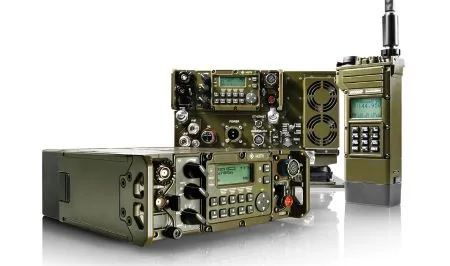
Communication Infrastructure
- Cell Transmission and Tower Electronics
- Fixed & Mobile Networks
- Satellite Technology
- Wireless Industrial and Commercial Phone Technology
- Broadband Equipment
- Fiber Optic Communication

Data Transmission and Networking
- High-Speed Routers and Switches
- Server Systems
- Data Centers
- Network Switching Equipment
- Broadband Modems
- Ethernet Devices
Security and Encryption
- Information Security Technology
- Military Communications Systems
- Encryption Devices
- Secure Communication Systems
- Network Firewalls

Voice and Video Communication
- PBX Systems
- Voice over IP (VoIP) Devices
- Video Conferencing Systems
- Unified Communication Systems
- Audio/Video Processing Equipment
- Intercom Systems
Specialized Applications
- Waveguide Grating Devices
- Signal Amplification Devices
- Airbag Deployment Systems
- Industrial Control Systems
- Sensing and Monitoring Equipment
- Medical Communication Devices
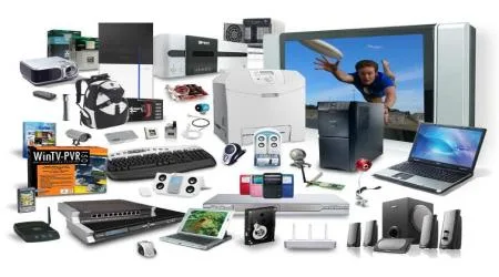
Consumer Electronics
- Smartphones and Tablets
- Internet of Things (IoT) Devices
- Home Networking Equipment
- Audio/Video Entertainment Systems
- Wearable Devices
- Gaming Consoles
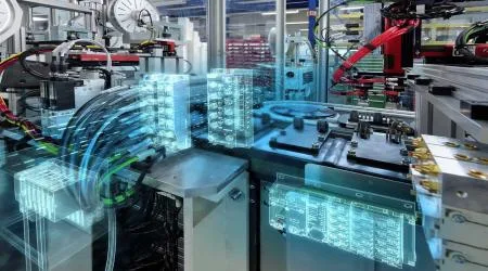
Communication PCB 5G construction features
Communication PCBs in 5G construction have significant features and requirements due to the high-speed and high-frequency nature of 5G technology. These features drive the demand for communication boards, especially in the construction of 5G base stations.
- Increased Base Station Quantity: The number of 5G base stations is much larger compared to current 4G base stations. Additionally, the deployment of micro base stations in blind spot areas further contributes to the demand for communication PCB boards.
- Industrial Control Environment: Communication PCBs are utilized in both wired and wireless communication equipment within industrial control environments. Wired communication equipment includes serial communication, professional bus-type communication, industrial Ethernet communication, and various communication protocol conversion equipment. Wireless communication equipment encompasses wireless APs, wireless bridges, wireless network cards, wireless lightning arresters, antennas, and other related devices.
- High-Frequency and High-Speed Requirements: The RF (Radio Frequency) part of communication PCBs operates at relatively high frequencies, while the baseband part handles digital signals with very high data rates. These characteristics impose stringent material requirements on the PCBs. Some components may also require boards with ceramic substrates to meet specific performance needs.
- Complex PCB Design and Processing: Communication PCBs often have dozens of layers, including through-hole plates. They may require a back-drilling process to ensure precise signal integrity and minimize signal reflection.
Highleap, as a trusted provider of telecommunications PCBs, understands the unique requirements of communication PCBs in 5G construction. We specialize in delivering high-quality PCB solutions that meet the demanding needs of high-speed and high-frequency communication systems.With our expertise in PCB design and manufacturing, we ensure that communication PCBs for 5G applications are designed to handle the increased base station quantity and provide optimal performance in industrial control environments. We incorporate advanced materials, including ceramic substrates when necessary, to meet the high-frequency and high-speed requirements of RF and baseband components.
Our experienced engineers and state-of-the-art facilities enable us to handle the complex design and processing needs of communication PCBs. With the ability to manufacture multi-layered PCBs with precision and efficiency, including through-hole plates and back-drilling processes, we ensure excellent signal integrity and minimize signal reflection.
Choose Highleap’s Communication PCB

Full Expertise
Highleap excels in communication PCBs, leveraging our expertise in high-speed and high-frequency designs to deliver optimized solutions for 5G construction and other applications.

Robust Supplier Network
Through our robust supplier network, we source high-quality materials and components, ensuring reliable and top-grade communication PCBs for various high-frequency applications.

Strict Quality Control
Our strict quality control processes guarantee exceptional performance and reliability, meeting the highest standards for communication PCBs’ signal integrity and durability.